\(f_\tau\) vs \(f_{max}\)
A device designer tweaks transistor and optimizes \(f_\tau\) whereas an IC designer tweaks circuit and optimizes \(f_{max}\). But why are there two different metrics, and which one should you use? What is the difference between \(f_\tau\) vs \(f_{max}\)? Let’s dive right in.
What is \(f_\tau\)?
The concept of \(f_\tau\) was introduced by device designers because it made sense to them. One is interested in finding out time that carriers take to travel across the device, one would take a look at transit-time \(\tau\) and inverse of that is transit frequency \(f_\tau\). Since this transit-time would be dependent on material properties (like mobility, diffusion constant, impurities added) and material geometry (like how long carriers need to travel), this is a great metric to express intrinsic speed of a device.
Why Use Current Gain for \(f_\tau\)?
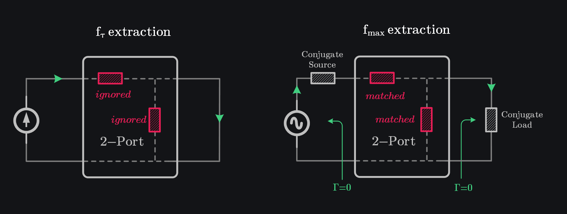
In circuit world, \(f_\tau\) is defined as frequency where current gain equals one. Why current gain? We are interested in transit-delay that is we send the charge in the device and record the time it takes for charge to come out. “Charge in” means you have to excite with current source so that any series parasitic don’t determine how much charge goes in as they would in case of voltage source. “Charge out” means you need to terminate the device with short circuit so that your charge does not gets lost in finite output impedance of device and you collect everything out you sent in. This charge in and charge out is basically current in and current out in circuit world. This is why we use current gain to determine \(f_\tau\).
Calculation of \(f_\tau\) from Small-Signal Model
Assume a generic small-signal model of a transistor. We have input series resistance represented by \(R_{in}\), input capacitance by \(C_{in}\), output resistance by \(R_{out}\), output capacitance by \(C_{out}\), feedback capacitance by \(C_{fb}\), and transconductance by \(g_m\) as shown in image below.
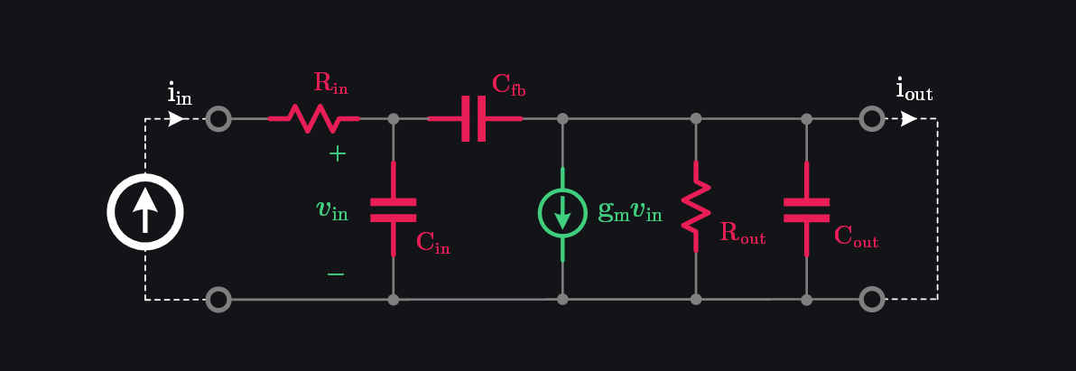
Since \(R_{out}\) and \(C_{out}\) are shorted, we can write output current as:
Since \(g_m \gg j\omega C_{fb}\) at most frequencies of interest:
Putting \(\beta=1\) to get \(f_\tau\):
Intuition Behind \(f_\tau\)
Above expression shows that \(f_\tau\) is directly proportional to \(g_m\) i.e., the higher the \(g_m\) the higher the \(f_\tau\) and inversely proportional to capacitances. Intuitively, we would expect the same i.e., transit frequency is inverse of delay, and delays are RC products, and we would want to minimize RC. Higher \(g_m\) means smaller diffusion resistance (\(\frac{1}{g_m}\)) and thus faster charging of capacitance \(C_{in}\) and \(C_{fb}\).
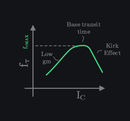
Note that \(f_\tau\) rises with \(g_m\) but then saturates at one point and drops afterwards. For BJT this happens because of physical limitation of base width which becomes bottleneck in delay after \(g_m\)-based delay is small enough and after that more secondary effects like Kirk effect start kicking in which start degrading \(f_\tau\) if \(g_m\) is increased any further. Also note that only \(C_{in}\) and \(C_{fb}\) need to be minimized but \(C_{out}\) plays no role (why would it? \(f_\tau\) conveniently ignores it by shorting the output).
Where \(f_\tau\) Falls Short
\(f_\tau\) gave us a sense of intrinsic speed of device – great for device designers. But, \(f_\tau\) has little meaning for circuit designers. We use it as a figure of merit to compare different transistors, but that is that. If \(f_\tau\) is say 300GHz, it does not mean the transistor can switch at 300GHz. Unlike the popular belief that \(f_\tau\) indicates the speed of digital circuits, it does not, or at best, does so poorly. \(f_\tau\) is a small-signal metric and ignores large-signal effects. The textbook expressions for \(f_\tau\) (what we also derived above) neglect large-signal delays. For example, when a BJT switches from ON to OFF, it moves through extreme regions of operation where charge removal, aka storage delay, is significant, yet small-signal \(f_\tau\) says nothing about it. Why? Turns out small-signal model completely ignores large-signal mechanisms of storage delay because afterall it was a “small” signal model. On top of that, \(f_\tau\) also ignores many parasitics that are crucial in practical circuit design. It focuses only on current gain. At the input, the device is excited with a current source, ignoring series parasitics. At the output, the device is loaded with a short circuit to collect all the current, disregarding shunt parasitics. But current gain is not everything! A device can still achieve power gain beyond \(f_\tau\), even though \(f_\tau\) seems to mark the end of the device by asserting unity current gain.
The Rise of \(f_{max}\)
\(f_\tau\) missing crucial parasitics is a significant lapse in the eyes of an IC designer. A new metric was needed that did not have shortcomings of \(f_\tau\) and could provide an idea of how high in frequency a transistor embedded in a real circuit could go. Since power gain is the real deal (current or voltage gain can be provided by passives too), RF designers were interested in knowing frequency at which power gain drops to unity. They called it \(f_{max}\). As maximum power gain occurs when device is conjugately matched, \(f_{max}\) definition naturally assumes that load and source impedances are conjugately matched at each frequency. This is fundamental difference between \(f_\tau\) vs \(f_{max}\).
Calculation of \(f_{max}\) from Small-Signal Model
Let’s terminate our small-signal model with conjugate load as shown in image below.

Lots of math coming. Don’t worry about the details—just know we’re finding where power gain drops to 1.
At high frequencies \(\frac{1}{\omega C_{in}} \approx 0\), therefore we neglect \(C_{fb}\) and write:
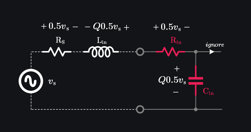
With conjugate matching, \(L_{in}\) will resonate \(C_{in}\) out and we will be left with \(R_{s}\) of source and \(R_{in}\) of device. Since \(R_s=R_{in}\) under matching, input voltage will be divided half and half between them. Input power delivered to device can then be given as:
At output side, we need to do little bit more manipulation. Consider this: we can resonate \(C_{out}\) with \(L_{out}\) but then should we choose \(R_L=R_{out}\)? After all, we chose \(R_S=R_{in}\) at input, so it would make sense to do similar at output? No. At input, we could neglect \(C_{fb}\) because \(C_{in}\) was much bigger. However, at output, the very fact of \(C_{in}\) being bigger will make \(C_{fb}\) “visible”. In other words, if \(C_{in}\) was small, \(C_{fb}\) would be terminated with higher impedance to ground thus drawing “ignorable” current from output, which is however not the case. If we cannot ignore \(C_{fb}\), we cannot use \(R_L=R_{out}\) as \(C_{fb}\) will draw current altering the impedance looking from the output of the device.
To figure out effective output impedance, excite the device with \(v_t\) and measure \(i_t\) which can be given as:
Compared with \(g_mv_{in}\), the current \(i_{fb}\) is much smaller, we can the write:
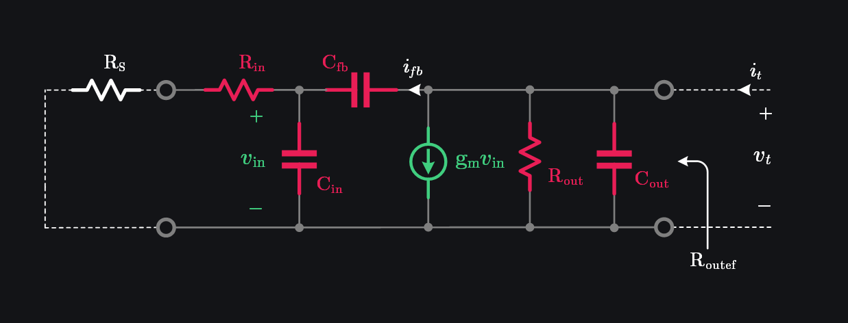
You just said we won’t ignore \(C_{fb}\) and now you ignore \(i_{fb}\). What is this? Good question. We did ignore a part of \(C_{fb}\) but a more important part of it is still there, hidden in \(g_mv_{in}\) because if we would have said \(C_{fb}\) is zero, then \(g_mv_{in}\) would have also been zero. We only said \(i_{fb}\) is zero which is OK otherwise we would start losing intuition and get lost in math.
As mentioned before, at high frequencies \(\frac{1}{\omega C_{in}} \approx 0\), therefore we can neglect \(R_{in}+R_S\), and write:
Putting this back in (3), we get:
Thus, impedance looking from output \(R_{out_{ef}}\) (and hence the \(R_L\) we should choose) can be given as:
Phew, now we can begin to compute power delivered to the load \(R_L\) as:
As for current division between \(R_{out_{ef}}\) and \(R_L\), it gets divided half and half because that is how we choose \(R_L\), we said \(R_{out_{ef}}=R_L\) under matching. Therefore,
Let’s figure out \(v_{in}\) now. We know input voltage \(v_s\) would be divided half and half between \(R_s\) and \(R_{in}\) as mentioned before. Now, recall that voltage across reactance is Q times the voltage across resistance. So, if \(R_{in}\) gets \(0.5v_s\), \(C_{in}\) would get \(0.5Qv_s\). Also, don’t confuse that sum of voltages has exceeded \(v_{in}\) because \(L_{in}\) will have exact same voltage as \(C_{in}\) but of opposite polarity and hence cancel out (fundamental property of resonance). OK, so we can write:
Putting this in (5), we get:
Let’s divide output power with input power to get power gain,
Therefore, the frequency at which power gain will be equal to one can be given as:
Intuition Behind \(f_{max}\)
It shows that \(f_{max}\) is proportional to \(f_\tau\) i.e., whatever in your device is limiting \(f_\tau\) will limit \(f_{max}\) too. On top of that, \(f_{max}\) is further limited by impedances device is terminated with.
- If \(R_{in}\) is zero, we would have no \(f_{max}\). This is important. \(R_{in}\) has such a crucial role that only if we could make it zero nothing else seems to matter. Device could work at any frequency. Why \(R_{in}\) is so important? Because it creates a series resonance circuit with \(C_{in}\). The voltage across \(C_{in}\) is what gets “trans-conducted”. As frequency is increased, reactance of \(C_{in}\) becomes smaller, and thus voltage across it reduces which eventually reduces output current \(g_m v_{in}\). Now here is the interesting fact: input power delivered remains same across frequency as per (2), it is only the voltage which goes down and brings output power down too. This also shows you that things don’t work with power. They work with voltages and currents.
- As for \(R_{L}\), we want to maximize it to maximize \(f_{max}\). This is because load is a shunt impedance. If you don’t want a shunt impedance to limit your speed, you would make it infinite (contrary to series impedance which you would make zero). In another sense, our output is a current source, so output power (\(I^2R\)) would be higher if load is higher (given that we can support voltage swings – because higher R would increase voltage at output, and you would either start getting clipped from power supply or run into reliability concerns from device)
Let’s expand (6). Putting back \(R_L\) from (3) in (6), we get:
If \(R_{out}\) is assumed high enough to be ignored, we get to the “textbook” expression for \(f_{max}\):
This again emphasizes the importance of \(R_{in}\) along with \(C_{fb}\). It pleads:
“Hey device designer, please don’t ignore \(R_{in}\) because I know in your metric it does not come up. But this is a huge trade-off for me. You (as BJT designer) would want to decrease base doping to reduce recombination and improve your \(f_\tau\) but this increases \(R_{in}\) and degrades my \(f_{max}\). Please consider this and choose an optimal doping because after all in real world it is \(f_{max}\) that we care about. \(f_\tau\) is just your thing.”
(Just to cover ground, can be skipped in first reading)
Calculation of \(f_{max}\) from Small-Signal S-Parameters
We came up with expression of \(f_{max}\) from small signal model. That was mainly for intuition and to understand what parameter plays what role. But man, did we make some assumptions? There were many, and if you were to calculate \(f_{max}\)from equations we derived above, you will likely not get anything precise – maybe just maybe a rough ballpark.
To extract accurate \(f_{max}\) from device, we can use s-parameters. Infact, s-parameters are often used in measurement-based \(f_{max}\) extraction because at high frequencies, currents and voltages are difficult to measure. It is difficult to create pure open and short loads. Everything behaves like a transmission line with reflections. S-parameters come very handy as they are easy to understand, easy to relate with gain, loss and power.
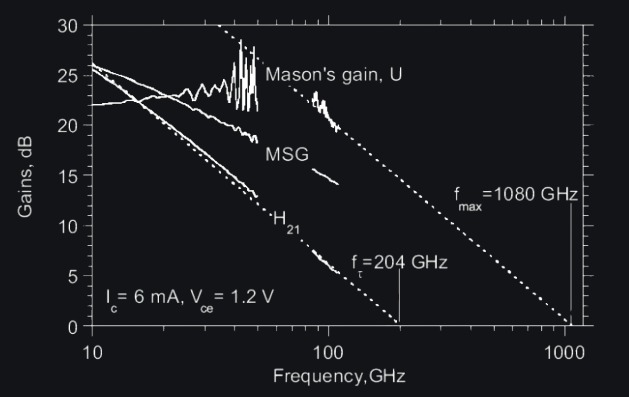
A bit confusingly, there exists two different ways to determine \(f_{max}\) from s-parameters:
1. via the maximum available gain The maximum available gain MAG is the gain of a two-port with conjugately matched input and output ports. If the scattering matrix \([S]\) of the device is known, MAG can be calculated: \[\large MAG = \left| \frac{s_{21}}{s_{12}} \right| (k \pm \sqrt{k^2-1})\] where \(k\) is Rollet’s stability factor. Unconditionally stable two ports have \(k > 1\). We note that MAG only exists as a real value for \(k ≥ 1\). This is significant limitation because indeed many transistors are not unconditionally stable over a wide frequency range. If MAG exists, however, it can be extrapolated to the frequency where MAG=1. This frequency is then called \(f_{max}\).
2. via Mason’s unilateral gain This definition circumvents the problem with the non-existence of MAG by defining \(f_{max}\) from the unilateral gain. The unilateral gain assumes that the two port is unilateralized i.e., \(s_{12} = 0\) which means or \(C_{fb}=0\), and the resulting two port is then conjugately matched at the input and output ports. The power gain can again be calculated from the scattering matrix of the original two port:\[\large U = \frac{1}{2} \frac{|\frac{s_{21}}{s_{12}-1}|}{k|\frac{s_{21}}{s_{12}-1}|-Re({\frac{s_{21}}{s_{12}-1}})}\] Extrapolating U to a frequency where U=1 again yields fmax — unfortunately, the two definitions will usually give a different \(f_{max}\), so it is important to note which method was used when comparing results.
Q: By the way, if you are conjugately matched at each frequency, that means you have resonated imaginary part out and are only left with real part, why does power gain drop at higher frequency then? There should be no frequency dependency or \(f_{max}\). One could theoretically go at as high frequency as one wants. What limits us? Hint: Series RC at input.
References
\(f_{max}\) derivation:
Microwave Engineering by David M. Pozar
S-parameters:
High Frequency Characterization of Transistors
Browse by Tags
RFInsights
Published: 01 April 2025
Last Edit: 01 April 2025