Device Physics Explained: Key Concepts for IC Designers
Chp.2: Energy Bands & Bandgap
To understand semiconductor device physics, we must first comprehend energy bands. Let’s go through the process step-by-step to learn how energy bands are formed and where the term bandgap originates from.
2.1 Discrete Energy Levels of Electrons Inside an Atom
We learned that electrons exhibit wave-like behavior and are confined within potential wells created by the atomic nucleus. This confinement, combined with their wave nature, results in electrons having discrete energy levels, meaning their energy is well-defined and does not assume arbitrary values.
These discrete levels arise because electrons can only “fit” into the potential well in specific, stable configurations, much like a rope fixed at both ends can only vibrate in certain standing wave patterns. Only specific wavelengths—and thus specific energies—are allowed, corresponding to these standing wave conditions.

It’s also interesting to note that if an electron were free (not bound within an atom), it would behave as a traveling wave instead of a standing wave. In that case, it wouldn’t be restricted to discrete energy levels but could possess a continuous range of energies. Therefore, it’s really the confinement that leads to discrete energy levels.
Q: Why does Energy of Electron Increase as It Moves to Higher Orbits?
As you move far from nucleus, electrons are less tightly bound, and their energy increases. How? Electrons have potential energy due to electrostatic attraction between proton and electron. Potential energy can be thought of “stored” energy or how much additional external energy is needed to remove or move something. Electrons in the first shell are tightly bound, meaning you need more external energy to remove them. As you move away from the nucleus, electrons are less tightly bound and easier to remove. In other words, the fact they can be easily removed with a little external energy indicates they already had higher energy.2.2 Formation of Energy Bands of Electrons
When many atoms come together to form a solid, the wave functions of their electrons interact, causing their discrete energy levels to split—some electrons take slightly higher energy, while others take slightly lower energy. As more atoms combine, these small splits create a continuum of closely spaced energy levels, forming an energy band. Although the band appears continuous, it’s actually made up of many discrete energy levels that are so close together they seem indistinguishable. In contrast, an isolated atom has clearly defined discrete energy levels without such splitting.
Intuitively, if two atoms were close enough and their electrons remained at the same energy level, it would violate the Pauli Exclusion Principle, which states that no two electrons can occupy the same quantum state. Therefore, the energy levels split, ensuring each electron has a unique quantum state.
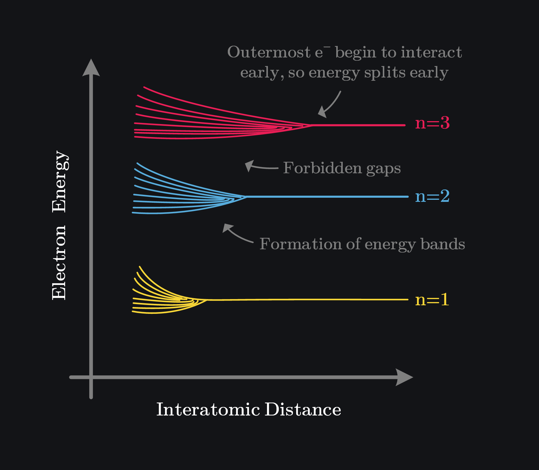
2.2.1 Valence and Conduction Bands
The two most important energy bands that determine most of a material’s electrical and chemical properties are the valence band and the conduction band. The valence band is formed by the interaction of the outermost (valence) electrons of atoms. It represents a continuum of energy levels derived from the valence shell of individual atoms.
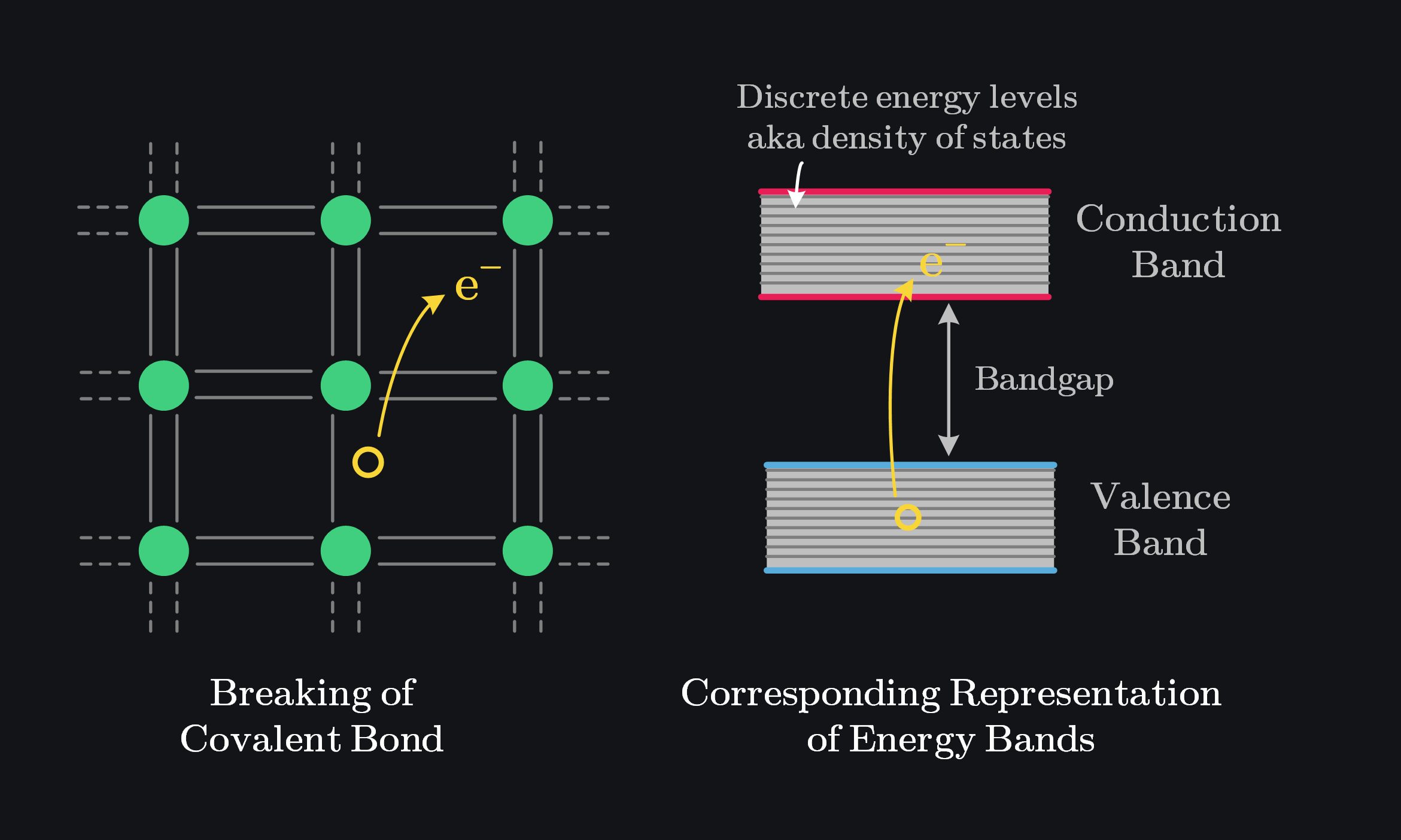
However, the conduction band is not simply the next atomic shell. It’s different. Conduction happens when electrons gain enough energy to break free from their atomic bonds, allowing them to move freely. When this happens, we say these electrons are in the “conduction band” (after all band is just a set of energies, so conduction band represent energies of those free electrons). Electrons here are delocalized, meaning they can move throughout the crystal lattice—they’re no longer bound to specific atoms but remain part of the material as a whole. This is distinct from ionization, where electrons are completely removed from the material.
For example, in Si, valence electrons occupy the 3rd shell (3s and 3p orbitals), but the conduction band is not the 4th shell. It is somewhere in between 3rd and 4th shell energy levels. To illustrate, the energy difference between the valence band and the conduction band in silicon is approximately \( 1.1 \, \text{eV} \), while the energy difference between the 3rd and 4th shells is much larger (\( 5-10 \, \text{eV} \)). Although the 4th shell exists, it does not significantly influence silicon’s electrical or chemical properties. The conduction band, however, is crucial for electrical conductivity.
2.3 Bandgap
The energy difference between the top of the valence band and the bottom of the conduction band is called as bandgap energy, denoted as \( E_g \). At absolute zero, all electrons occupy the lowest available energy states, meaning the valence band is completely full, there is no conductivity, hence no concept of conduction band. At temperatures above absolute zero, thermal energy excites some electrons, enabling them to break free from bonds, we depict it as if an electron jumped across the bandgap into the conduction band, making the material conductive.
2.3.1 Band Structure (E-k Diagrams)
The real band structures are quite complicated – not as shown in above image with conduction and valence band being straight lines. As electrons move through crystal lattice, they experience different potentials in different directions because the spacing and arrangement of atoms vary with direction (and hence “different” pulls from nuclei around). We use a vector k (aka wavevector) to represent the direction and wavelength of the electron in the crystal lattice and plot electron energy E along k to show how E will change as electron moves in particular direction. Such plots are known as E-k diagrams. Usually [100], [110], and [111] directions in k-space are shown because they represent high-symmetry paths where the energy bands often have special features (e.g., minima, maxima, or saddle points). Note k-space is bit different from Miller indices (which are used to define planes within a crystal), however purpose is similar that is to define direction. Here’s how to interpret k-space directions:- [100]: Goes from the center (k=0, Gamma point) to the center of a face (X-point).
[110]: Goes from the center (k=0, Gamma point) to the midpoint of an edge (K-point).
[111]: Goes from the center (k=0, Gamma point) to a corner (L-point).
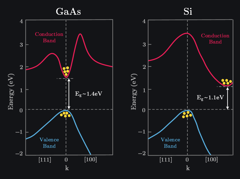
Q: Why do Electrons Settle at Min of Conduction Band?
In above image, we saw that electrons were settled at min of conduction and holes at max of valence band. Remember that electrons first fill the lowest energy shell in an atom and then above? Systems in nature tend to evolve toward states of lower energy because these states are more thermodynamically stable. When an electron in conduction band has higher energy, it experiences scattering events (lattice vibrations, impurities etc.), loses its energy and settles down to lowest possible energy level. Similarly, when an electron recombines with hole, it fills lower energy holes first, as a result holes appear to congregate at the valence band max, because that’s where the highest-energy vacant states exist.
2.3.2 Direct and Indirect Bandgap
When the minimum of the conduction band and the maximum of the valence band occur at the same momentum (k-vector) in the band structure, we call it direct bandgap because this allows electron in conduction band to directly recombine with hole in valence band (by emitting photon). This makes them useful for optical applications like LED and lasers. GaAs is a direct bandgap material.
Now that we have an understanding of how energy bands and gaps are formed, we are ready to calculate the number of ‘free electrons’ in a semiconductor that contribute to its conductivity.
Browse by Tags
RFInsights
Published: 07 Feb 2025
Last Edit: 07 Feb 2025