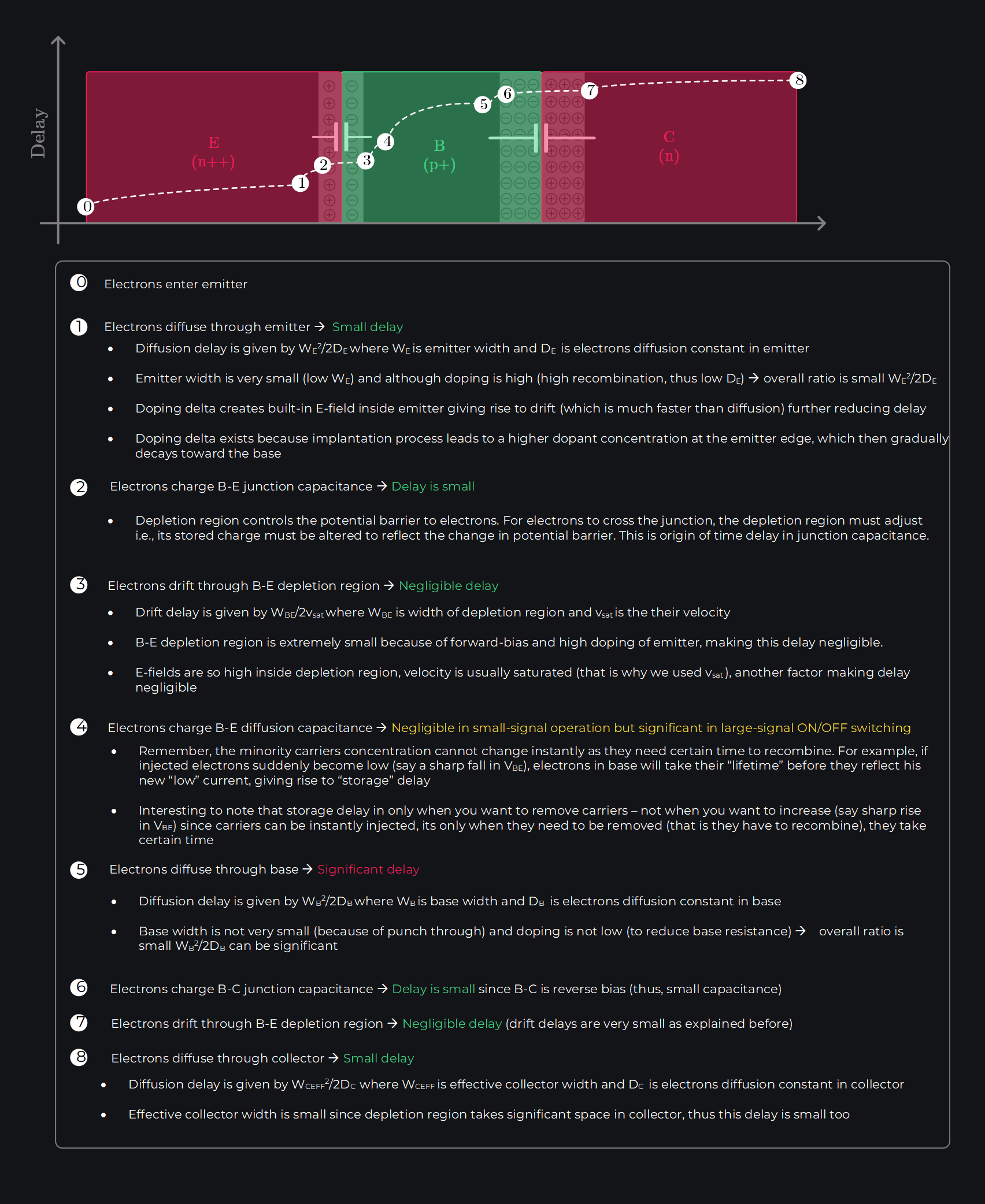
How to Design a High-Performance BJT: Key Concepts for Analog and RFIC Designers
8.1 Why Do I Care? I Am a CMOS Guy
Why should I care about BJTs? This is the CMOS age. If you design full TX/RX chains in industry, chances are you’re using CMOS. But if you look at dedicated RF front-end blocks (like LNAs and PAs) you’ll notice they often use non-CMOS tech. Sometimes SOI, but more often, HBTs (a variant of BJTs). Turns out, BJTs have survived the test of time.
It wouldn’t be an exaggeration to say BJTs are still the best transistors for RFIC applications, offering higher \(f_{max}\) and \(f_\tau\) than CMOS. And let’s be real, CMOS hasn’t been making big moves beyond 22nm in terms of RF performance.
- Folks on Reddit? They blame quantum tunneling.
- Folks at ISSCC? They say it’s because channel length isn’t shrinking anymore and metal/contact parasitics are piling up as we cram things tighter and tighter.
Either way, CMOS \(f_{max}\) isn’t improving the way we hoped. Meanwhile, BJTs are accelerating, pushing towards \(f_{max}\) in the THz range. And here’s the thing: junctions are everywhere whether you use CMOS or non-CMOS. If you really want to understand how transistors work, BJTs are the best place to start. They show you how to use junctions cleverly, and once you get BJTs, you get a much deeper feel for device physics.

In last post, we learned how a BJT works. Let’s dig into details and see how key metrics like gain, \(f_{max}\), breakdown and linearity are traded off in BJT design.
8.2 Current Flow in BJT
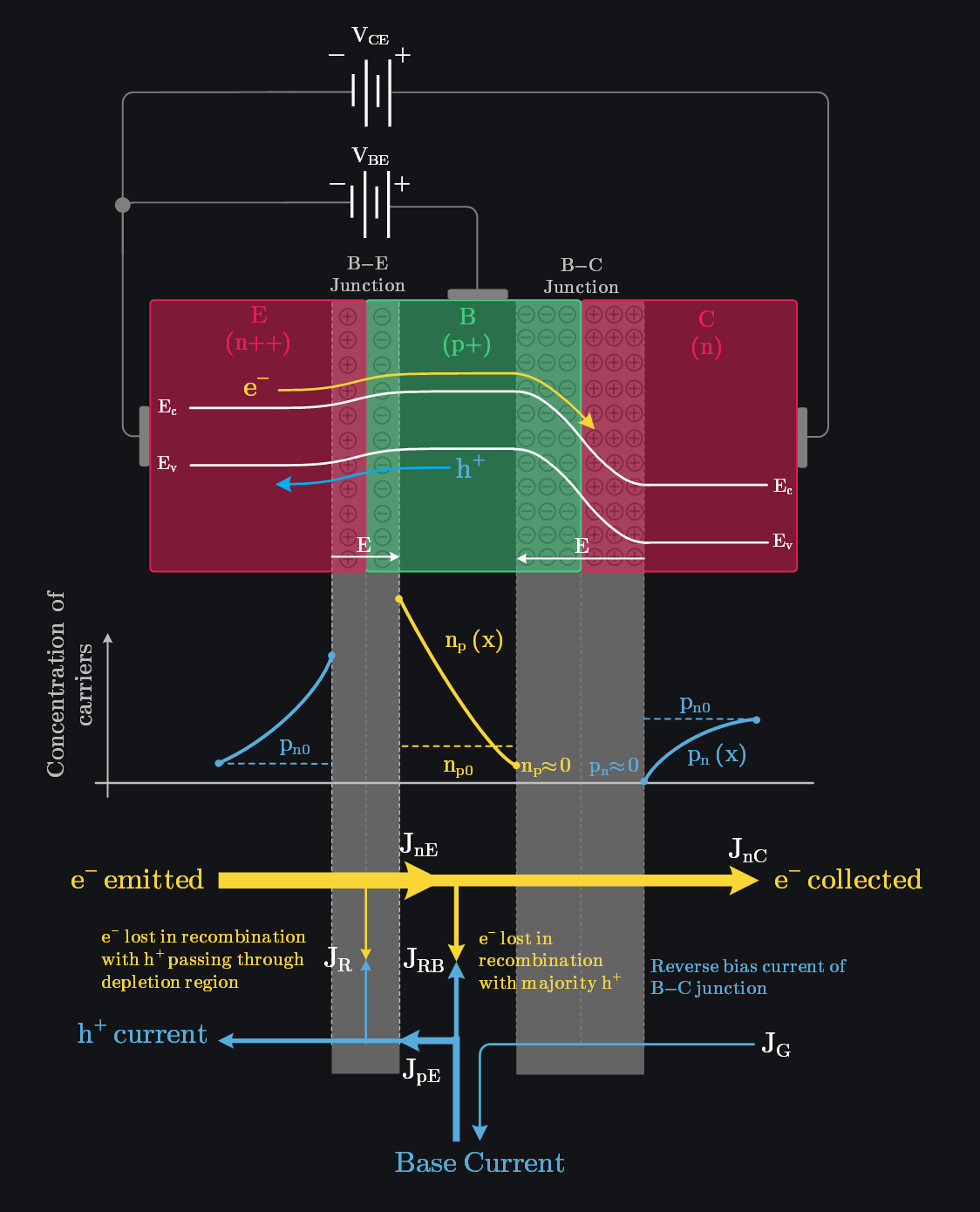
Let’s understand how current flows in BJT before we dive deep. The base–emitter (B–E) junction is forward biased which injects electrons from the emitter across the B–E junction into the base. These injected electrons create an excess concentration of minority carriers in the base. The base–collector (B–C) junction is reverse biased, so the minority carrier electron concentration at the edge of the B–C junction is ideally zero. The large gradient in the electron concentration means that electrons injected from the emitter will diffuse across the base region into the B–C space charge region, where the electric field will sweep the electrons into the collector. This completes the flow of current as shown in the image below. Let’s understand different components of current first.
8.2.1 Carrier Concentrations Explained
- \(n_p(x)\): This represents the minority electrons injected from the emitter into the base. The sharp concentration gradient means they diffuse rapidly, recombining with majority carrier holes as they move. By the time they reach the collector side, their concentration is nearly zero—this tells us how aggressively the reverse-biased collector-base junction sweeps them into the collector, generating the collector current.
- \(p_n(x)\): This represents the minority holes injected from the base into the emitter. Again, there’s a steep gradient, so they decay quickly as they diffuse towards the emitter contact, recombining with majority electrons along the way. This recombination is responsible for the base current.
- \(p_n(x)\) at the collector side: Near the depletion edge, the hole concentration is essentially zero—another sign of how effectively the reverse-biased junction sweeps away any holes, contributing to the reverse-bias leakage current.
8.2.2 Current Components Explained
Collector and base current consist of many components. Let’s breakdown them. The current densities are defined as follows:
- \(J_{nE}\) : Minority carriers electrons injected from emitter to base due to forward bias B-E junction
- \(J_{nC}\) : Minority carriers collected at collector due to reverse bias B-C junction
- \(J_{RB}\) : The difference between \(J_{nE}\) and \(J_{nC}\), which is due to the recombination of excess minority carrier electrons with majority carrier holes in the base. The \(J_{RB}\) current is the flow of holes into the base to replace the holes lost by recombination.
- \(J_{pE}\) : Minority carriers holes injected from base to emitter due to forward bias B-E junction
- \(J_R\) : Due to the recombination of carriers in the forward-biased B–E junction.
- \(J_G\) : Generation current due to reverse bias of B-C junction.
8.3 Optimizing BJT Current Gain: Key Contributing Factors
To maximize BJT current gain, we need to:
- Collect all the minority carriers injected by emitter without getting them lost on the way through recombination. In circuit terms, we call it collector current should be equal to emitter current i.e., \(\alpha=\frac{J_{nC}}{J_{nE}}=1\)
- Minimize hole injection from base to emitter and reverse bias currents of B-C junction as they do not contribute to collector current. In circuit terms, we say base current should be zero i.e., \(J_{RB}=J_{pE}=J_{R}=J_{G}=0\)
These goals can be achieved if we can make \(\alpha=\frac{I_C}{I_E}\) aka common base current gain to be unity. This will ensure that \(\beta=\frac{I_C}{I_B}\) aka common emitter current gain is maximized since they are related as:
\(\alpha\) can be broken down into three components which all needs to be unity in order to make \(\alpha\) unity.
Let’s understand these components one-by-one:
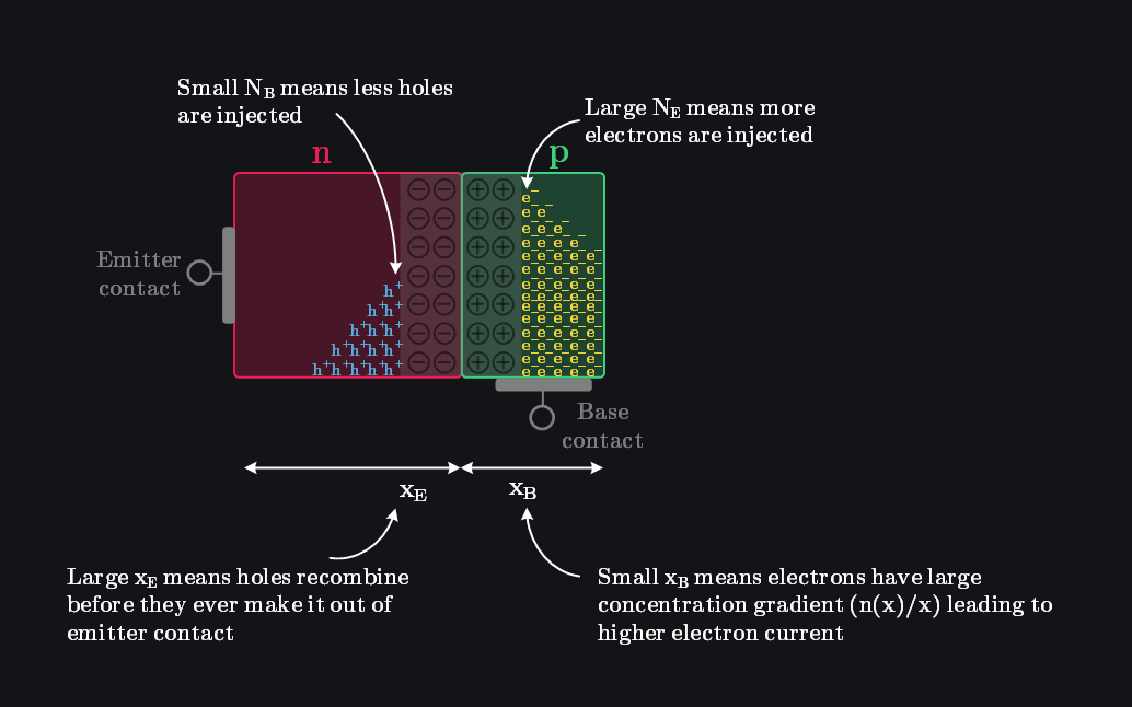
8.3.1 Emitter Injection Efficiency \(\gamma\)
The emitter injection efficiency factor \(\gamma\) takes into account the minority carrier hole diffusion current in the emitter. This current is part of the emitter current, but does not contribute to the transistor action in that \(J_{pE}\) is not part of the collector current. It is defined as:
Putting in expression for diffusion current and some mathematical manipulations will reveal that we can write \(\gamma\) as [1]:
where,
- \(N_E\) and \(N_B\) are the impurity doping concentrations in the emitter and base, respectively
- \(D_E\) is the diffusion constant of holes in emitter
- \(D_B\) is the diffusion constant of electrons in base
- \(x_B\) and \(x_E\) are the base and emitter physical widths respectively
Above equation suggests, for the emitter injection efficiency to be close to unity:
The emitter doping must be much larger than the base doping. This ensures that far more electrons from the n-type emitter are injected into the base than holes from the p-type base into the emitter.
- The emitter width must be larger than base width. A large emitter width ensures that any holes injected from the base will recombine with majority carrier electrons before they reach the emitter contact. This means less hole current escaping through the emitter contact, which is crucial because what matters is the current at the contacts that external circuit has to supply or absorb. Inside the semiconductor, plenty of charge movement happens, but if it doesn’t require an external supply, we don’t care. Our ultimate goal is to minimize the base current, reducing the load on the driving circuit, and reducing hole current escaping through emitter contact means reducing current through base contact.
- For the same reason, we want the hole diffusion constant \(D_E\) in the emitter to be small. A smaller diffusion constant means less hole diffusion current, further reducing the unwanted hole injection from the base.
Q: Can We Keep Increasing Emitter/Base Doping Ratio to Improve Emitter Injection Efficiency?
As emitter doping increases, bandgap narrows. This happens because the large concentration of dopant atoms disrupts the perfect periodicity of the silicon lattice, giving rise to a band tail instead of a sharply defined band edge. This is as if the bandgap is reduced which is detrimental as it lowers built-in potential (remember built-in potential is proportional to bandgap energy). This reduced barrier allows electrons to be injected from base to emitter and degrades emitter injection efficiency – the very thing you were trying to improve by increasing emitter doping. So, your improvement start to cencel itlsef if you go too far.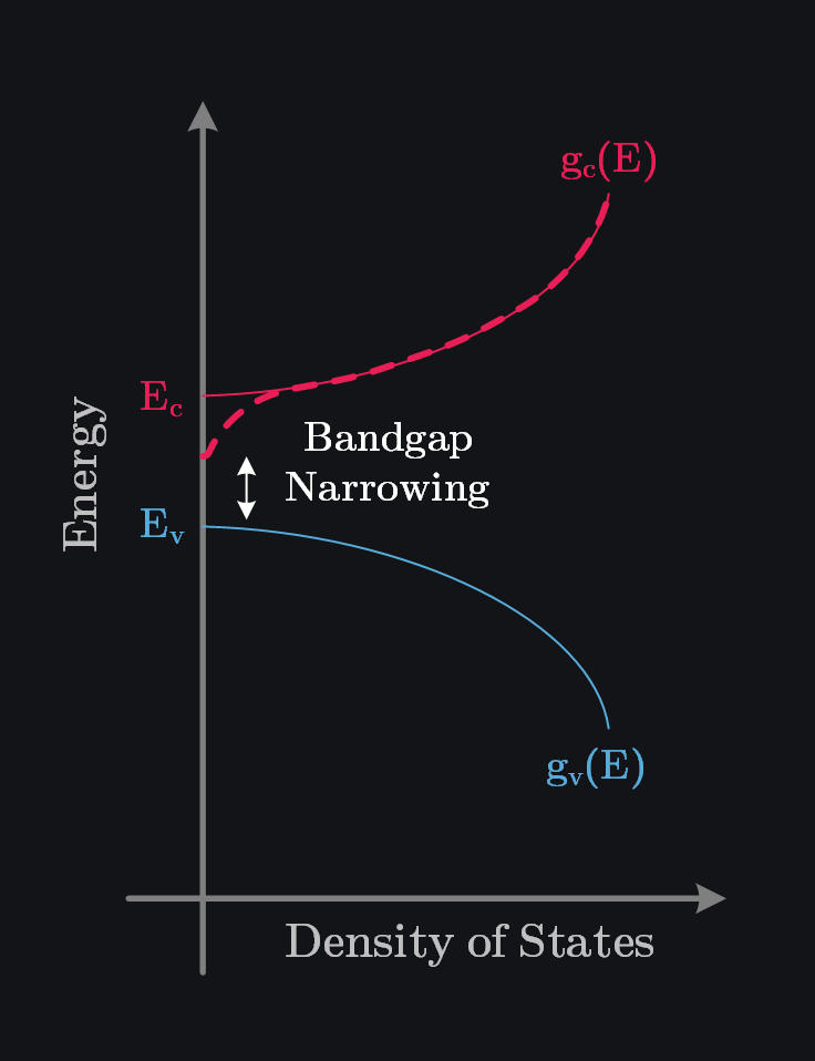
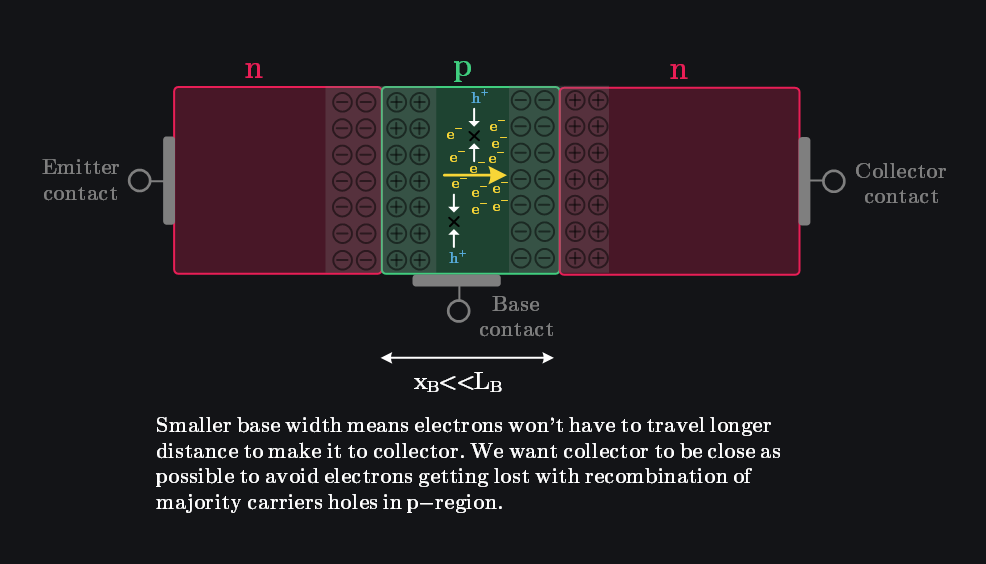
8.3.2 Base Transport Factor \(\alpha_T\)
The base transport factor \(\alpha_T\) takes into account any recombination of excess minority carrier electrons in the base. Ideally, we want no recombination in the base. It is defined as:
Putting in expression for diffusion current and some mathematical manipulations will reveal that we can write \(\alpha_T\) as [1]:
where \(L_B\) is diffusion length. Above equation suggests, for the base transport factor to be close to unity, the base width must be much smaller than diffusion length. This makes sures minority carriers don’t spend too much time passing through base and getting lost in recombination. For \(x_B<<L_B\), we may expand the cosh function in a Taylor series such that
8.3.3 Recombination Factor \(\delta\)
The recombination factor \(\delta\) takes into account the recombination in forward biased B–E junction. The current \(J_R\) contributes to the emitter current but does not contribute to collector current. Recombination factor can be defined as:
It can be further simplified to, as detailed in [1]:
where \(c\) is some constant which depends on base width, doping, lifetime etc. We don’t need to worry about it. What we learn is that the recombination factor is a function of the B–E voltage. As \(V_{BE}\) increases, the recombination current becomes less dominant, and the recombination factor approaches unity.
8.4 Numerical Example: Designing for High BJT Current Gain
Let’s take an example to make sense of it all. Say, we want current gain \(\beta=100\), then \(\alpha=\frac{\beta}{1+\beta} =0.99\). If we also assume that \(\gamma=\alpha_T =\delta\), then each factor would have to be equal to 0.9967 in order that \(\beta=100\).Assume \(D_E=D_B\) and \(x_E=x_B\) for simplicity. To get \(\gamma\) to be \(0.9967\), we need:
This shows that emitter doping concentration must be 300 times larger than the base doping concentration to achieve a high emitter injection efficiency.
Assume \(L_B=1\mu m\). To get \(\alpha_T\) to be \(0.9967\), we need:
This shows that base width has to be very small to achieve a high base transport factor.
Assume \(c=1000\), to get \(\gamma\) to be \(0.9967\), we need:
This example demonstrates that recombination factor may become dominant limiting factor if bias voltage is lower than 0.654V.
8.5 Optimizing BJT for \(f_\tau\) and \(f_{max}\): Key Contributing Factors
Our analysis of current gain did not consider frequency effects. We focused on current collection by making sure all the injected current is collected. Next, we may ask how long does it take to collect the injected carriers because that will ultimately determine how fast can we switch the device. The time carriers take to traverse the device is known as transit time \(\tau\), and corresponding frequency is known as transit frequency \(f_\tau\). They are related as:
Note that there is \(2\pi\) factor because delay is inverse of angular frequency, on the other hand time periods are inverse of linear frequency.
\(\tau\) can be broken down into three main components:
- Diffusion delays (significant)
- Can be derived to be \(\dfrac{W^2}{2D}\) where \(W\) is width (distance that carriers have to travel) and \(D\) is the diffusion constant [2]
- ⬇️\(W\) \(\implies\) ⬇️diffusion delay
- ⬇️ Doping \(\implies\) ⬇️ impurities scattering \(\implies\) ⬆️\(\mu\) \(\implies\) ⬆️\(D\) \(\implies\) ⬇️ diffusion delay
- Drift delays (negligible)
- Can be derived to be \(\dfrac{W_{DR}}{2v}\) where \(W_{DR}\) is width of depletion region and \(v\) is the speed [2]
- ⬇️ \(W_{DR}\) \(\implies\) ⬇️ drift delay
- ⬆️ \(v\) \(\implies\) ⬇️ drift delay (usually electric fields are very high in depletion region and velocities always reach fixed \(v_{sat}\))
- Storage delays (negligible in small-signal operation)
- In saturation both the E-B and B-C junctions are forward biased. This means that carriers (electrons in an NPN) are injected from the emitter into the base without an efficient “sweeping” mechanism at the collector to remove them. As a result, extra (excess) minority carriers build up in the base region. This stored charge must be removed when turning the transistor OFF, which incurs additional delay called as storage delay. This delay is negligible in small-signal operation since transistor operates in active region (E-B forward bias, and B-C reverse) with very small swings.
- For example, storage delay in base is given by \(\dfrac{Q_B}{I_B}\) where \(Q_B\) is total charge stored in base and \(I_B\) is the base current.
- ⬇️ \(W_B\) \(\implies\) ⬇️ charge stored \(\implies\) ⬇️ storage delay
- ⬆️\(I_B\) \(\implies\) ⬆️ fast removal of charge \(\implies\) ⬇️ storage delay (trade-off with \(\beta\) which wants lower \(I_B\))
- ⬆️ Doping \(\implies\) ⬆️ recombination \(\implies\) ⬇️ storage delay (trade-off with \(\beta\) which wants lower doping)
We can then write total transit time as:
where,
- \(\tau_E\) is emitter diffusion delay
- \(\tau_{EB}\) is E-B junction drift delay \(\implies\) negligible (drift is way faster than diffusion)
- \(\tau_S\) is E-B storage delay \(\implies\) negligible (small-signals do not introduce excess charge carriers)
- \(\tau_B\) is base diffusion delay
- \(\tau_{BC}\) is B-C junction drift delay \(\implies\) negligible (drift man)
- \(\tau_C\) is collector diffusion delay \(\implies\) negligible (since most of collector is taken by B-C depletion region where things are drifting, little is left for diffusion)
Since most components are negligible, transit time is often approximated as:
Image below provides step-by-step account of these delays as carriers (electrons in our example) encounter while they travel from emitter to collector.
8.5.1 Linking Transit Frequency\(f_\tau\) to Unity Current Gain \(\beta=1\)
As the frequency increases, this transit time \(\tau\) can become comparable to the period of the input signal. At this point, the output response will no longer be in phase with the input and the magnitude of the current gain will decrease. One would then want to define a frequency where collection is 3dB less than injection. Therefore, we can re-write \(\alpha\) as:
where \(\alpha_0\) is DC common-base current gain and \(f_\tau\) is 3dB cutoff frequency related to \(\tau\) as we know \(f_\tau=\dfrac{1}{2\pi\tau}\)
This shows that at \(f=f_\tau\;\), \(\beta=1\). This is the origin for the definition of transit frequency, where we say \(f_\tau\) is unity (common-emitter) current gain frequency or 3dB common-base current gain frequency.
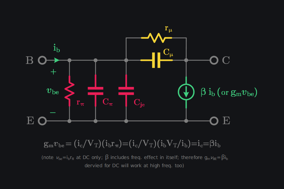
8.5.2 Translating BJT Device Physics into a Small-Signal Model
So far, we’ve examined \(f_\tau\) from a purely device-level perspective. Now, let’s develop a small-signal circuit model to bridge the gap between the device and circuit domains.
- Diffusion Delay results from the physical distance that carriers travel due to slower diffusion (slower because carriers meet recombination on their way + diffusions are naturally slower than drifts). This delay is modeled by time-constant \(r_\pi C_\pi \). Similarly, one can add \(r_\mu\) to reflect diffusion resistance of B-C junction but usually it is quite large and can be ignored (since B-C junction is reverse-biased i.e., OFF)
Let’s drive \(C_\pi\) in terms of transit-time. Say, it takes time \(\tau\) to transit charge \(Q\) from emitter to collector (i.e., \(\tau\) includes all diffusion delays base, emitter, collector). We can then write:
Also note that, this only expresses \(C_\pi\) in terms of \(\tau\), it does not mean that diffusion delay only results from \(C_\pi\) and \(r_\pi\) has no role. \(r_\pi\) is hidden inside \(g_m\) as we know \(\beta=g_mr_\pi\).
- Junction Delay arises from the fact that the potential barrier in the depletion region cannot instantly respond to the applied external potential. This is because the charge density within the depletion region needs time to adjust. This “not being able to instantly respond to potential” behavior characteristic of a capacitor, therefore it is modelled as capacitances \(C_{je}\) & \(C_\mu\).
- Depletion Delays are not included in the model since they are negligible
- Storage Delay is not included in the model since storage is mainly a large signal behavior, its effects are negligible in small-signal operation.
8.5.3 Calculation of \(f_\tau\) from Small-Signal Model
Since we are interested in current IN (injection) and current OUT (collection), we can short-circuit output (C-E) to collect all the current irrespective of load. The base and collector currents can be written as:
Ignoring 1 as sum of other terms in denominator is much bigger than unity at high frequencies. Also, ignoring \(j\) to arrive get magnitude:
Putting \(\beta=1\):
This means \(\beta\) can also be written as:
Let’s figure out \(f_\tau\) in terms of \(\tau\), consider from Eq (2):
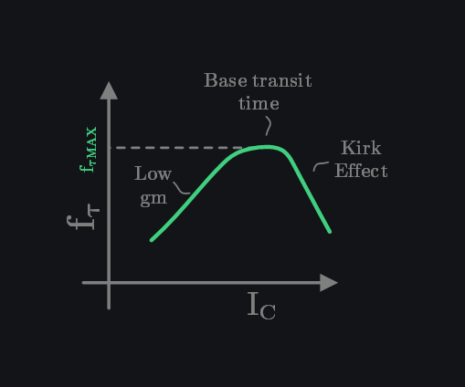
This shows dependence of \(f_\tau\) on \(g_m\). At lower currents, \(g_m\) is low, the second term in denominator is much bigger than \(\tau\), hence \(f_\tau\) increases with collector current. Physically this means, when \(g_m\) is low it takes more time to charge junction capacitances which increases the delay. At medium currents the depletion capacitance term becomes smaller than \(\tau\), and hence \(f_\tau\) ceases to rise with collector current, reaching peak \(f_{\tau MAX}\), and is given by:
This means peak \(f_\tau\) is limited by diffusion delay which as mentioned before is dominated by base transit time.
At high collector currents the cut-off frequency decreases markedly due to Kirk effect. Therefore, it is important to select collector current correctly: too low or too high both not good, there is an optimal for peak \(f_\tau\).
8.5.4 \(f_\tau\) vs \(f_{max}\)
While \(f_\tau\) is a great metric for device designers, it is not very meaningful circuit designers. For example, series parasitic at input of device and shunt parasitic at output of device are ignored in \(f_\tau\) whereas they can seriously degrade operating frequency in a real circuit. \(f_{max}\) was introduced to account for such parasitics and is more realistic measure of how high in frequency a device can really go. We have a dedicated post on \(f_\tau\) vs \(f_{max}\) here, where we derive \(f_{max}\) to be:
\[\LARGE {\textcolor{#40CE7F} {f_{max} = \sqrt{\frac{f_\tau}{8 \pi r_b C_{\mu}}}}}\]
here \(r_b\) is the series resistance at input before \(r_{\pi}\) as shown in image below. This shows that \(r_b\) is so crucial to \(f_{max}\). If \(r_b\) were zero, we would get infinite \(f_{max}\) even though \(f_\tau\) would remain same. \(r_b\) originates from finite base doping (device designer controls this) and base contact resistance (layout designer can mitigate this). Base doping is dominant source of \(r_b\) as base is lightly doped to inject less holes current and thus increase \(\beta\). This shows there is direct trade-off between \(\beta\) and \(f_{max}\).
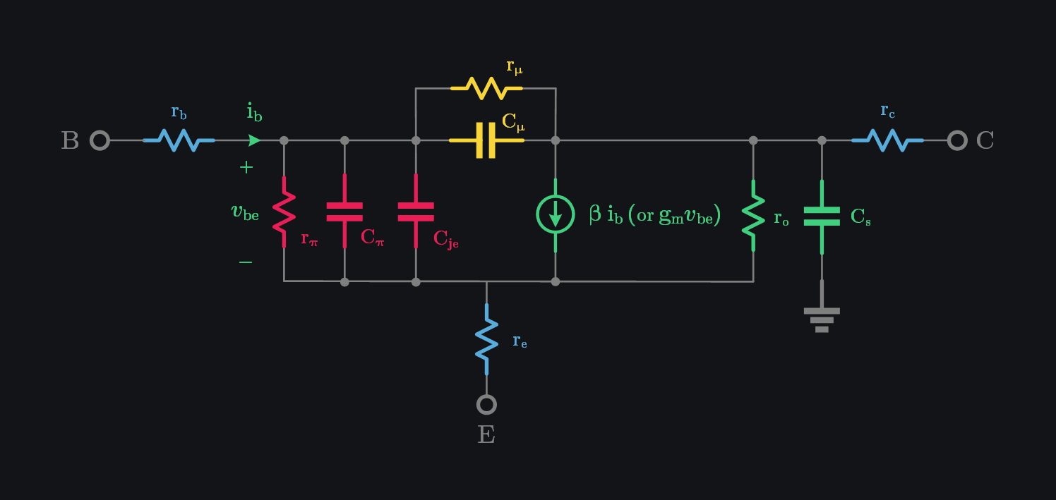
\(r_b, \; r_c\) and \(r_e\) are base, collector and emitter resistances from contact and finite dopings, \(r_o\) is from base-width modulation and \(C_s\) is capacitance between collector and substrate as collector sits on top of substrate as show in cross-section here.
8.6 BJT High-Voltage Performance: Breakdown Considerations
We know a PN junction breaks down when reverse bias voltage is increased. A BJT has two PN junctions:
- B-E junction: Since it is forward biased, there is no breakdown concern.
- B-C junction: Since it is reverse biased, it breaks down just like a regular PN junction diode does (avalanche, Zener) + there are some additional considerations (punch-through, common-emitter vs common-base breakdown etc.) which we will discuss below.
8.6.1 Zener Breakdown
Zener breakdown happens when doping concentrations are high. Since base and collector are lightly doped, this is usually not a concern for BJT.
8.5.2 Punch-Through
We learned that a reverse bias to a PN junction causes the depletion region to extend. When BJT is in forward active mode, B-C junction is reverse biased. This causes B-C junction to extend. If reverse bias is increased, there comes a time that junction has extended so much that it occupies whole basewidth and joins up B-E depletion region. The emitter and collector are then connected together by a single depletion region, as shown in image. This is known as punch-through, and when it occurs B-E potential barrier is lowered which results in very large current flow between emitter and collector. Intuitively, this can be understood as collector strong electric field now reaching the base and pulling the electrons from emitter as if B-E forward bias was increased and henc more current flows for same B-E voltage. While not a breakdown in the traditional avalanche sense, the electrical behavior is similar to junction breakdown. Punch-through sets a fundamental limit on how much the base width of a bipolar transistor can be scaled down. A thinner base increases gain and speed but also lowers the breakdown voltage, making the device more susceptible to punch-through.
- ⬆️ Base-width to keep base wide enough to prevent overlap \(\implies\) ⬆️ Punch-Through Voltage but ⬇️ \(\beta\)
- ⬆️ Base doping to make depletion region narrower \(\implies\) ⬆️ Punch-Through Voltage but ⬇️ \(f_\tau\)

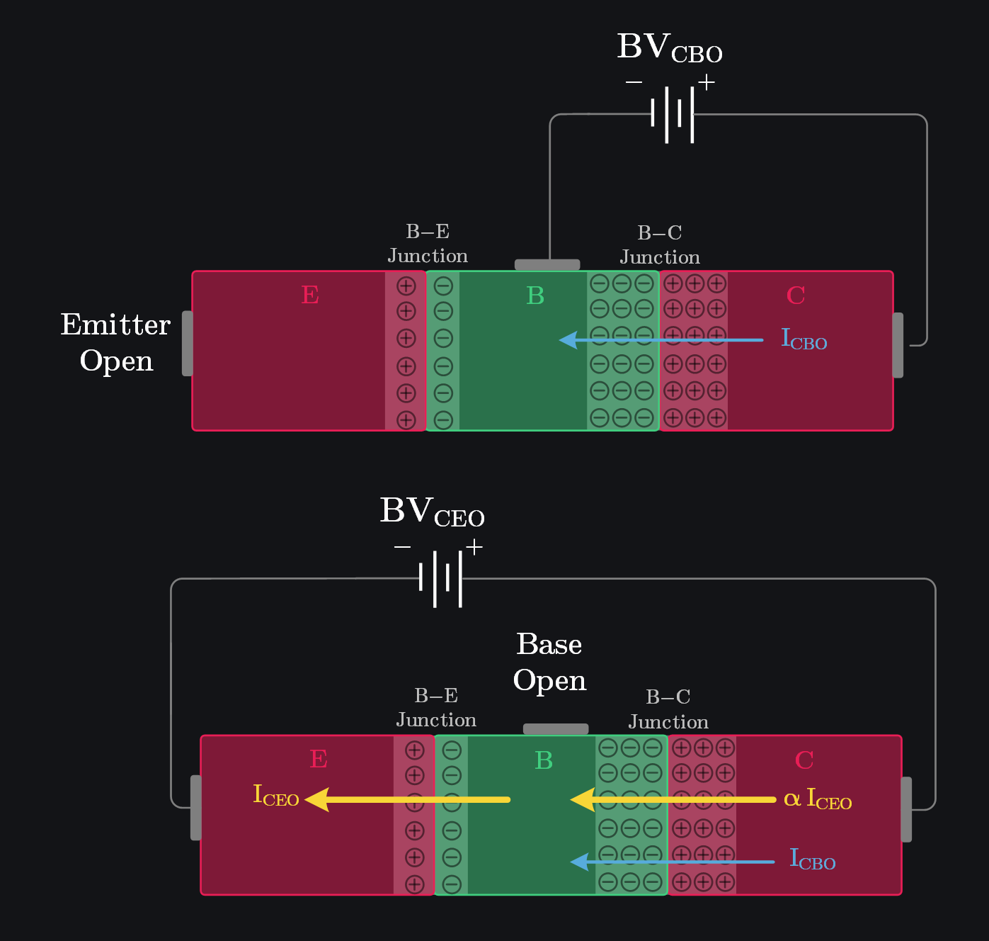
8.5.2 Avalanche Breakdown (\(BV_{CEO} \;\&\; BV_{CBO}\))
Avalanche multiplication or impact ionization is by far the most common breakdown mechanism in junctions. In bipolar transistors, the avalanche breakdown voltage depends on the base termination impedance. If base is terminated with low impedance as in common-base connection where base is grounded, the breakdown voltage obtained is the same as that of a normal PN junction. If base is terminated with higher impedance as in common-emitter connection, the breakdown voltage is considerably lower, as shown in image. Therefore, in practice, two breakdown voltages are reported:

\(BV_{CBO}\) (Collector–Base breakdown with emitter open):
- The emitter is open, so the transistor cannot conduct.
- You’re simply reverse-biasing the B-C junction.
- In this case, the junction behaves like a regular reverse-biased diode, and breakdown occurs only when the electric field becomes strong enough to trigger avalanche.
\(BV_{CEO}\) (Collector–Emitter breakdown with base open):
- The base is open, and the emitter is connected.
- A small reverse leakage current \(I_{CBO}\) flows from collector to base due to minority carriers (e.g., holes from collector to base for an NPN BJT).
- Since the base is floating, this current raises its potential slightly above the emitter, effectively forward-biasing the B–E junction.
- This turns the transistor ON and causes a much larger collector current \(I_{CEO}\), which is approximately \(\beta\) times \(I_{CBO}\).
- This amplified current feeds into the reverse-biased B–C junction, injecting a much larger number of carriers into the high-field region.
- Avalanche breakdown can be triggered either by a very strong electric field or by a very high density of carriers.
- In this case, the large number of carriers provided by transistor action accelerates the breakdown process, allowing it to occur at a lower voltage than \(BV_{CBO}\) case — hence \(BV_{CEO}<BV_{CBO}\)
- The very transistor action that you want (current gain) now got you and reduced the breakdown. It can be derived that:
\[\large \textcolor{#40CE7F}{BV_{CEO} = \frac{BV_{CBO}}{\beta^{\frac{1}{n}}}}\]
where n is an empirical constant, usually between 3 and 6.
Trade-off between Gain and \(BV_{CEO}\)
Above equation shows that the common emitter breakdown voltage \(BV_{CEO}\) is inversely proportional to the common emitter current gain \(\beta\) of the transistor. There is therefore a trade-off between gain and breakdown voltage. Clearly a high gain and a high breakdown voltage cannot be obtained simultaneously, so a compromise must be reached between reasonable values of gain and breakdown voltage.
- ⬇️ Collector doping to widen depletion region and hence reducing electric fields \(\implies\) ⬆️ \(BV_{CEO}\) ⬇️ \(f_{max}\) by increasing \(r_c\)
- ⬇️ Base doping to widen depletion region and hence reducing electric fields \(\implies\) ⬆️ \(BV_{CEO}\) ⬇️ Punch-Through Voltage
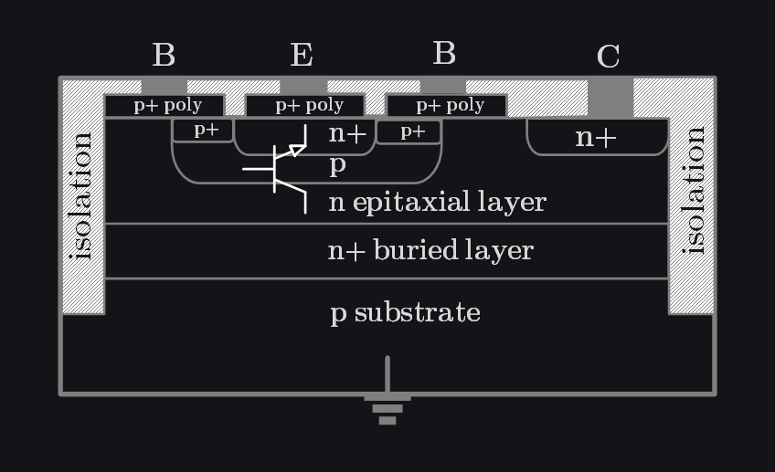
8.6 Cross Section of BJT
The BJT is built on a p-type substrate which serves as the reference potential (e.g., ground). An n⁺ buried layer is placed on top of the substrate to reduce the collector’s series resistance; without it, the relatively lightly doped collector region would suffer from excessive voltage drop and delays. Above the buried layer is an n-type epitaxial layer, which is grown specifically to form the collector region with controlled doping. The p-type base region is diffused or implanted into this epitaxial layer, and an n⁺ region is subsequently introduced to create the emitter. Heavily doped p⁺ and n⁺ regions at the surface make low-resistance contacts to the base, emitter and collector. The p⁺ polysilicon seen in the diagram is commonly used as an intermediary between metal and semiconductor contacts; it provides a high doping source, prevents unintentional junction formation, easier to pattern etc. etc. Finally, isolation regions on either side electrically separate this transistor from other devices on the chip, ensuring proper functionality and preventing unwanted current flow.
8.7 Second Order Effects
8.7.1 Quasi-Saturation
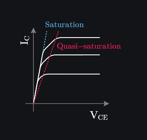
Quasi-saturation is an effect that occurs at high currents due to the internal collector resistance \(r_c\) of the transistor. It occurs when the voltage drop across the collector resistance is large enough to forward bias the B-C junction. The quasi-saturation is seen as a soft transition into the saturation region of the transistor’s IV curve. Its effect is greater at higher collector currents, because the voltage drop across the internal collector resistor is larger.
8.7.2 Current Crowding
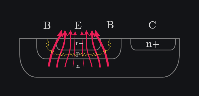
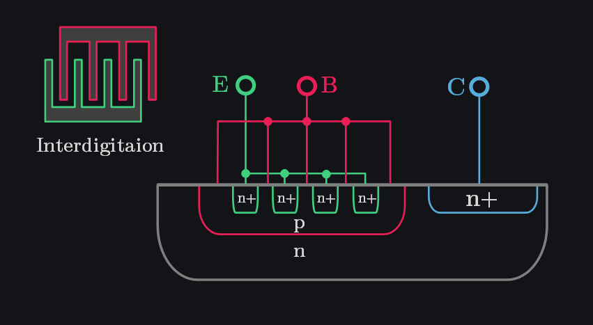
At high currents there can be a significant voltage drop across the intrinsic base resistance \(r_b\) of a transistor due to the lateral flow of base current from the base contact. As a result of this voltage drop across the intrinsic base resistance, the potential in the base close to the base contact is higher than that away from the base contact. Consequently, the B-E junction is more forward biased at the edge of the emitter that is closest to the base contact. This effect is known as current crowding since the current crowds to the edge of the emitter that is closest to the base contact. The larger current density near the emitter edge may cause localized heating effects as well as localized high-injection effects. If a bipolar transistor is required to deliver a high current, it is therefore necessary to maximize the emitter perimeter for a given emitter area. This can be done by partitioning the emitter into narrow emitter fingers and interdigitation.
8.7.3 Kirk Effect
When the mobile charge in the B–Cdepletion region exceeds the fixed ionized donor charge, the net space charge is reduced, weakening the electric field in the collector. As a result, the neutral base region extends into the collector, effectively widening the base. This phenomenon, known as base widening or base pushout or the Kirk effect, occurs at high current densities and degrades transistor performance by increasing base transit time and reducing current gain.
8.7.4 High Level Injection
As \(V_{BE}\) increases, the injection of electrons from the emitter into the base becomes more intense. At sufficiently high bias, the concentration of these injected minority carriers (electrons in the p-type base) can become comparable to the base’s majority carrier concentration (holes). When this happens, the base region starts to behave more like an intrinsic region, disrupting the normal operation of the BJT. This shift in carrier dynamics reduces the emitter injection efficiency, because the advantage of the heavily doped emitter over the lightly doped base is diminished. As a result, fewer of the total carriers crossing the E-B junction come from the emitter, degrading transistor gain.
8.7.5 Thermal Runaway
Assume you have a big BJT device. It is like as if you have connected many smaller ones in parallel. When several junctions operate in parallel, a slight temperature increase in one can lower its built-in potential, causing it to conduct disproportionately more current than its neighbors. This localized current hogging can drive the junction into high-level injection, further increasing its temperature and leading to a destructive feedback loop. To mitigate this effect, resistors are often placed in series with the base (called base-blasting) or emitter (called emitter blasting). These resistors help to drop a portion of the voltage externally, ensuring that no single junction is forced to handle excessive current, thereby maintaining uniform current distribution and preventing thermal runaway and subsequent damage.
8.7.6 Base-Width Modulation
The base width in a BJT is not fixed; it depends on the B-C voltage, since the width of the space charge region extending into the base varies with this voltage. As the reverse bias across the B-C junction increases, the depletion region widens further into the base, effectively narrowing the neutral base width. This reduction in base width steepens the gradient of the minority carrier concentration across the base, which in turn increases the diffusion current and hence the collector current. This phenomenon is known as base width modulation, or Early effect. Ideally, the collector current should remain constant with changes in B-C voltage, resulting in perfectly flat output characteristics and infinite output resistance. However, due to the Early effect, the collector current shows a slight dependence on the collector voltage, leading to a nonzero slope in the output characteristics, and thus finite output resistance known as \(r_o\).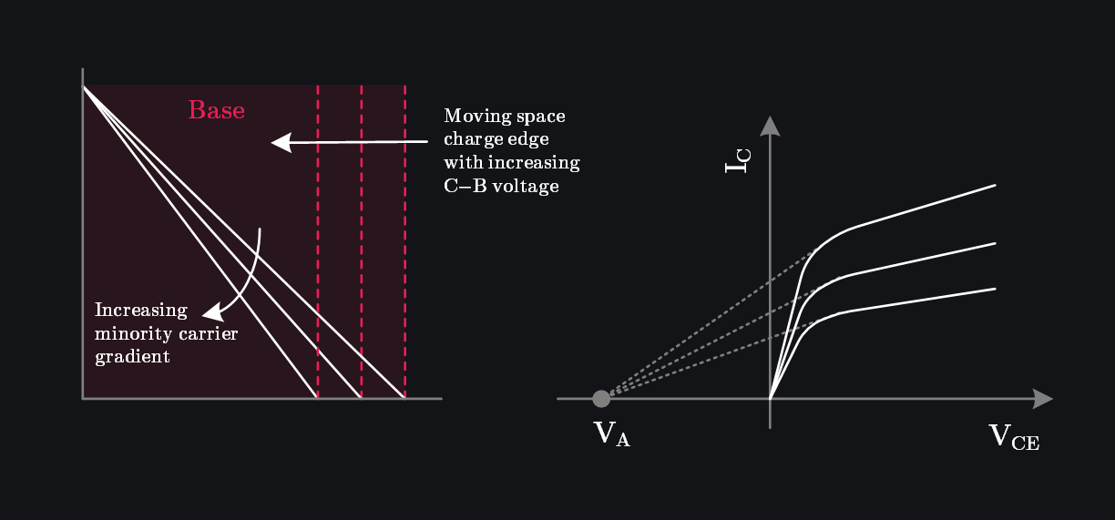
8.8 Linearity Consideration
| Effect Name | What it Varies | Explanation | Optimization/Mitigation Techniques |
|---|---|---|---|
| Base Width Modulation | Output resistance \(r_o\) | The B–C depletion region expands and contracts as output voltage (and hence B–C voltage) changes. This leads to change in base-width which results in change in collector current. | Shield your \(g_m\) transistor from voltage swings e.g., by using cascode. |
| Exponential Current | Transconductance \(g_m\) | The exponential I–V relationship of the B–E junction causes \(g_m\) to vary steeply with \(V_{BE}\), making it very non-linear. | Use degeneration, feedback, feedforward, and pre-distortion techniques as listed here. |
| High Injection Effects | Current gain \(\beta\) | At high current densities, the injected minority carrier concentration can rival the majority, disrupting exponential behavior and reducing gain. | Optimize layout e.g., use interdigitation to mitigate current crowding. |
| Junction Capacitance Variation | Input/output capacitances | Capacitance of the junctions changes with applied voltage, affecting frequency response and introducing phase distortion. | Use feedback neutralization techniques and reduce device size. |
| Series Resistance Variation | Output current and region of operation | Series resistances create current-dependent voltage drop. For example, if the collector draws a large current, the drop across \(r_c\) can be so high to put the device into saturation. | Optimize geometry and contact layout. |
| Thermal Runaway | Gain and current | Localized heating lowers \(V_{BE}\), causing that device to draw more current, which increases heating further, leading to high injection and potential damage. | Use base or emitter ballasting resistors. |
| Impact Ionization | Current multiplication and breakdown | High electric fields can generate additional carriers, resulting in nonlinear multiplication and possible breakdown. | Operate below breakdown limits. |
8.9 Summary of Trade-offs in BJT Design
Note: In device context, term width is used so we kept it but for circuit designers its actually “length” (something that comes fixed from foundry). So, table below is mainly from device designer perspective, we (circuit designers) don’t control these things.
| Parameter | Effect on Current Gain | Effect on High Frequency Performance | Effect on Breakdown Voltage |
|---|---|---|---|
| Base Width 🔼 | 🔽 (more recombination lowers gain) | 🔽 (longer transit time slows switching) | 🔼 (wider base reduces punch-through risk) |
| Emitter Width 🔼 | 🔼 (improves injection efficiency) | 🔽 (increased diffusion delay) | minimal direct effect |
| Collector Width 🔼 | little direct effect | 🔽 (longer carrier path increases delay) | 🔼 (spreads electric field, improving breakdown) |
| Base Doping 🔼 | 🔽 (more hole injection/recombination) | 🔽 \(f_\tau\) (reduced diffusion constant hampers speed) 🔼 \(f_{max}\) (reduced base series resistance) | 🔽 (narrower depletion region lowers breakdown voltage) |
| Emitter Doping 🔼 | 🔼 (enhances injection efficiency) | some improvement seen as \(\beta\) increases but bandgap narrowing offsets gains | 🔽 (bandgap narrowing lowers built-in potential which affects indirectly, there is no direct effect since breakdown is mostly B-C junction phenomena) |
| Collector Doping 🔼 | minimal effect on gain | little effect on carrier transit | 🔽 (higher doping increases electric field intensity, lowering breakdown voltage) |
Browse by Tags
RFInsights
Published: 13 April 2025
Last Edit: 13 April 2025