Device Physics Explained: Key Concepts for IC Designers
Chp. 4: Carrier Transport
There are mainly two ways charge carriers transport in semiconductors: 1) Drift, and 2) Diffusion.
4.1 Drift
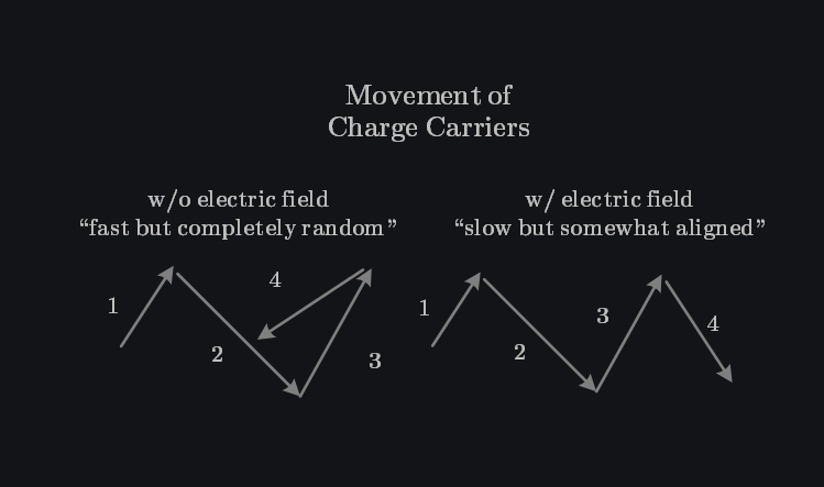
The transport of carriers due to an electric field is called drift. When you apply voltage across a material, it generates an electric field \(E\) which accelerates charge carriers to move in (or against) the direction of \(E\). Charges themselves have very high instantaneous velocity (~\( 10^5-10^6 \) m/s) due to thermal energy but it is random in all directions, resulting in net zero flow of current. Applied electric field gives them direction but frequent collision with lattice and impurity atoms reduces the speed to (~\(10^{-4}-10^{-2} \)m/s). On average, we get a constant velocity \(V_{drift}\) given as:
\[V_{drift}\, = \, \mu E\]
where \(\mu\) is called mobility.
Q: Why Does Mobility Degrades with Higher Temperature?
Mobility is hindered by two effects: 1) Lattice scattering and 2) Ionized impurity scattering
Mobility due to lattice scattering decreases as the temperature increases. Intuitively, we expect the lattice vibrations to increase as the temperature increases, which implies that the probability of a scattering event also increases, thus decreasing mobility.
Mobility due to impurity scattering increases as the temperature increases. This is because when the temperature increases, the random thermal velocity of a carrier increases, reducing the time the carrier spends in the vicinity of the ionized impurity atom. The less time spent in the vicinity of a coulomb force, the smaller the scattering effect and the larger the mobility.
In lightly doped semiconductors, lattice scattering dominates, and the carrier mobility decreases with temperature. In general, the trend is decrease in mobility with higher temperature and with higher doping.
Q: Why Do Electrons have Higher Mobility than Holes?
Mobility is approximately three times higher for electrons than for holes in silicon. Holes are nothing but absence of electrons. At the end of day, it is electrons that move whether its n-type or its p-type material. Why do we then think that p-type materials are slower, or holes have lower mobility? This is because in n-type materials, electrons are in conduction band and drift freely under electric field. In p-type materials, electrons hop from one atom to another, filling a hole while creating another hole at the previous location. Every time an electron hops, it takes time, as it is actively filling gaps left by the missing electrons, thereby degrading mobility. There are more factors at play such as effective mass of hole being higher than electron, band structure of conduction vs valence being different etc. etc. that can answer this question but “hopping” is an easier escape.
Q: Why Does Mobility Degrade at Higher Electric Field?
Mobility is not constant and decreases at higher electric fields. This is because higher \(E\) accelerates carriers more, increasing their energy and making collisions with the lattice (phonon scattering) more frequent. These collisions reduce the net drift velocity (and hence mobility) and prevent carriers from accelerating indefinitely in a high electric field. As a result, the carrier velocity eventually reaches a maximum value, known as the saturation velocity. The drift velocity of electrons in Si, for example, saturates at approximately \(10^7\) cm/s at an electric field of approximately 30 kV/cm. If the drift velocity of a charge carrier saturates, then the drift current density also saturates and becomes independent of the applied electric field.
4.1.1 Drift Current
Drift current arises from the carrier transport under an applied electric field and consists of two components:
- Electron current – Electrons in the conduction band move opposite to the direction of the applied electric field.
- Hole current – Holes in the valence band appear to move in the direction of the electric field. This occurs because electrons in the valence band shift between atoms, making it seem as if the holes themselves are moving.
It is important to recognize that electron movement occurs in both the conduction and valence bands—not just in the conduction band, as is commonly assumed when discussing electrical conduction. The movement of electrons and holes can also be understood through the bending of energy bands under the electric field.
Additionally, hole current does not imply recombination. Recombination is a distinct process where a free electron in the conduction band loses energy and fills a hole in the valence band, reducing the number of free carriers. In contrast, drift simply governs the movement of existing carriers without altering their overall concentration.
We can now define total drift current density as the sum of electron and holes current:
\[J_{drift}\, = q(\mu_nn+\mu_pp)E\]
where:
- \(q\) is the elementary charge,
- \(n\) is the concentration of electrons,
- \(\mu_n\) is the electron mobility,
- \(p\) is the concentration of holes,
- \(\mu_p\) is the hole mobility,
- \(E\) is the applied electric field.
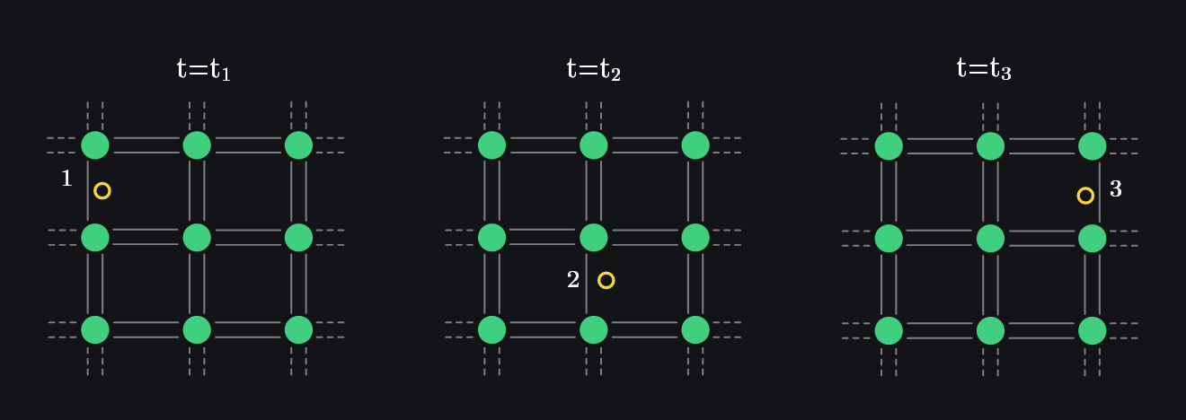
Q: Why Don’t Electrons and Holes Drift Current Cancel?
One confusion that we might develop is that electrons and holes appear to be moving in opposite direction of applied electric field. Shouldn’t they cancel? No. On macroscopic level, it is always electrons that move since hole is just a concept. Image below shows how a hole from “left to right” is actually an electron moving from “right to left”. Therefore, even though it might appear that hole moved in the direction of electric field, it was actually electron which moved against the direction of electric field, overall adding to the electron current (which was already in direction opposite to the electric field).
4.1.2 Conductivity
The current density can also be written as:
\[J_{drift}\, = q(\mu_nn+\mu_pp)E = \sigma E \]
where is \(\sigma\, = q(\mu_nn+\mu_pp)\) the conductivity of the material. The equation shows conductivity depends on two factors: 1) how many charge carriers are there, 2) how mobile are they.
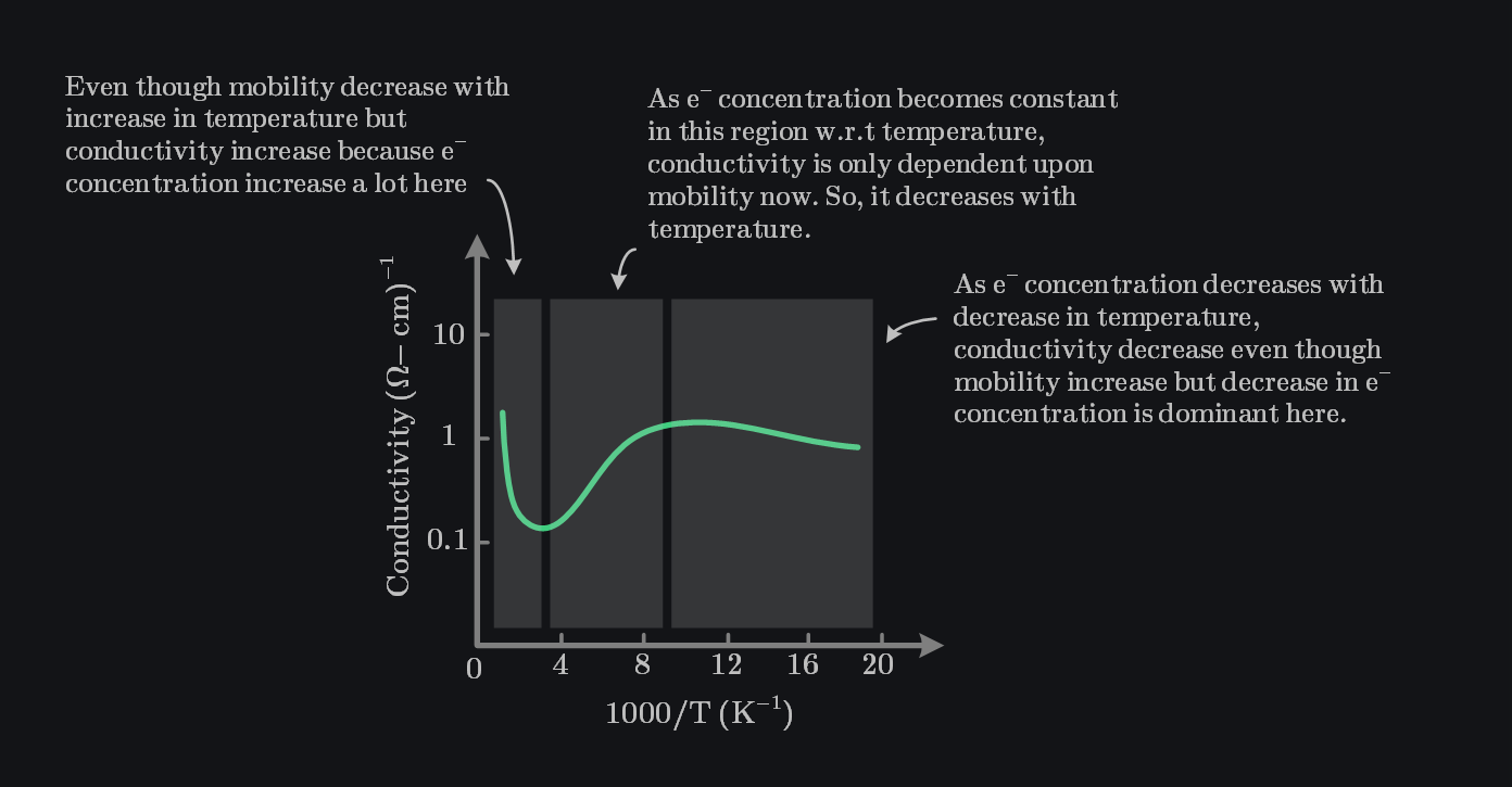
Above image shows the conductivity of Si as a function of inverse temperature for the case when number of donor atoms are ~\(10^{15}\,cm^{-3}\). In the mid-temperature range, or extrinsic range, we have complete ionization—the electron concentration remains essentially constant (remember it is dominated by doping in this region). However, the mobility is a function of temperature, so the conductivity varies with temperature in this range. At higher temperatures, the intrinsic carrier concentration increases and begins to dominate the electron concentration, therefore we see conductivity rising with temperature. In the lower temperature range, freeze-out begins to occur; the electron concentration decreases therefore we see conductivity decrease as temperature decrease.
4.2 Diffusion
Carrier transport can happen in absence of electric field as well when there is a difference in concentration. Charge carriers flow from high concentration to low concentration region until uniformity is achieved. This movement is called diffusion and resulting current is called diffusion current. Diffusion current is proportional to concentration gradient i.e., higher concentration difference (n) between distance (x) leads to higher diffusion current, and can be derived to be:
where:
- \(q\) is the elementary charge,
- \(n\) is the concentration of electrons,
- \(D_n\) is the electron diffusion constant,
- \(p\) is the concentration of holes,
- \(D_p\) is the hole diffusion constant,
Q: Why may Electrons and Holes Diffusion Current Cancel?
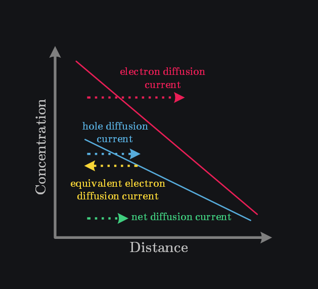
We saw in equation above that electrons and holes diffusion current have opposite sign that is net diffusion current could be lower. Look at image below. It shows if you introduce electron and hole concentration gradient at same place, electrons will move from left to right giving electron diffusion current and holes will also move from left to right giving hole diffusion current. However, if you convert holes to equivalent electrons movement that means in fact it is again electrons that are moving but from right to left to fill holes, then you can “assign” negative sign to this hole current. Overall, you would see electrons moving from left to right (electron diffusion current) and electrons moving from right to left (holes diffusion current), thus both completely cancelling each other out (if concentration gradients and diffusion constants were same).
Q: Why Do Things Diffuse?
Diffusion is a natural phenomenon: nature likes randomness and high entropy (meaning more disordered system) because maintaining order requires more energy. Things want to be in equilibrium because at equilibrium system has distributed energy in the most statistically likely way. Therefore, charge carriers also diffuse until equilibrium is achieved.
Q: Why is Diffusion Length and Minority Carrier Lifetime?
- Minority Carrier Lifetime (\(\tau\)): This is the average time a minority carrier (electron in a p-type region or hole in an n-type region) exists before recombining with a majority carrier. A longer lifetime means that the carrier persists for a greater duration before being annihilated through recombination.
- Diffusion Length (\(L\)): This represents the average distance a minority carrier travels before recombining. It depends on both the carrier’s lifetime and how easily it diffuses through the material. Diffusion length and lifetime can be related as : \(L = \sqrt{D \tau}\)
For majority carriers, because they are so abundant, recombination doesn’t significantly affect their overall concentration in the same way. Thus, we don’t worry about majority carrier lifetime.
4.3 Einstein Relation
When you take a non-uniformly doped semiconductor in equilibrium, there is no net current, so you can equate diffusion and drift currents (happening internally because of doping gradient), you will come up with this: \[\frac{D_n}{\mu_n}=\frac{D_p}{\mu_p}=\frac{kT}{q}\]This shows that diffusion coefficient and mobility are not independent parameters (how can they be? they both relate to movement of charges which is hindered by lattice scattering and ionized impurity scattering, as discussed earlier). This relation between the mobility and diffusion coefficient is known as the Einstein relation.
Browse by Tags
RFInsights
Published: 18 Feb 2025
Last Edit: 18 Feb 2025