Device Physics Explained: Key Concepts for IC Designers
Chp. 5: PN Junction
The PN junction is the cornerstone of all semiconductor devices. Once you truly understand its behavior, the rest of device physics becomes much more intuitive. In this post, we aim to provide a concise yet insightful glimpse into:
- Carrier distributions (majority/minority, injection, diffusion)
- Current mechanisms (diffusion, drift, recombination)
- Depletion region behavior (width, electric field, potential)
Let us start from how these junctions are formed.
5.1 Formation of PN Junction
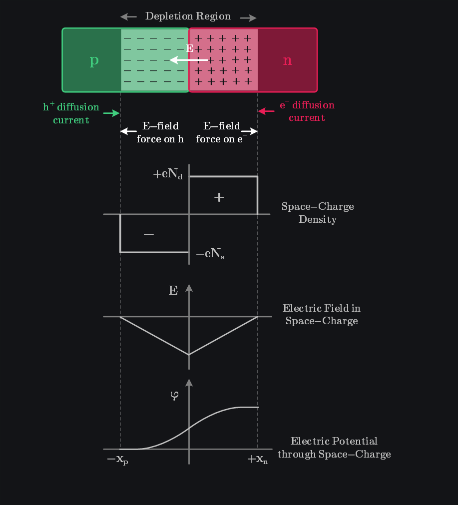
An n-type material has high concentration of electrons, while a p-type material has a high concentration of holes. We know that. Now, when we connect these two materials, the sharp concentration gradients lead to diffusion currents: electrons diffuse from the n-type region to the p-type region, and holes diffuse from the p-type region to the n-type region. As electrons leave the n-region, they leave behind positively charged donor ions. Similarly, as holes diffuse out of the p-region, they expose negatively charged acceptor ions.
Over time, the immediate vicinity of the junction becomes depleted of free carriers, as carriers near the junction diffuse away before those from the farther edges. This carrier-depleted region is known as the depletion region. The net positive charge in the n-region and the net negative charge in the p-region create an electric field across the depletion region, directed from the positive charges (n-side) to the negative charges (p-side). This electric field exerts a force on electrons and holes in a direction opposite to that of diffusion, giving rise to a drift current. The junction reaches equilibrium when the electric field becomes strong enough to completely counteract the diffusion currents. At this point, the drift and diffusion currents are equal in magnitude and opposite in direction, effectively canceling each other out.
The existence of this electric field implies that a potential difference has developed across the junction, known as the built-in potential, which can be calculated as:
where \(N_A\) & \(N_D\) are number of acceptor and donor atoms added to p and n-type materials respectively. Basically, it says built-in potential is a function of how much you doped the material (i.e., \(N_A\) & \(N_D\)) but not very strong (e.g., a tenfold increase in \(N_A\) or \(N_D\) would lead to only 60mV increase in \(V_{bi}\) at room temperature)
The image below shows a uniformly doped PN junction (therefore, we see constant space-charge density throughout the depletion region). The potential through space-charge region (\(\phi\)) and the electric field (\(E\)) are also illustrated. Notice that \(E\) peaks at the junction center because this is where the strongest attraction between opposite charges occurs. The charge density within the depletion region is uniform, resulting in a linearly changing \(E\) with distance. Since \(\phi\) is integration of \(E\) over distance, linear variation of \(E\) results in quadratic variation of \(\phi\).
Why Does the Built-in Potential Decrease with Temperature?
The above equation might initially suggest that the built-in potential \( V_{\text{bi}} \) increases with temperature. However, in reality, it decreases. This occurs because the intrinsic carrier concentration \( n_i \) increases exponentially with temperature, which counters the linear temperature dependence seen in the equation. Intuitively, as temperature rises, \( n_i \) increases in both the n-type and p-type materials, which means minority carriers are no longer much in minority now since intrinsic carrier concentration (i.e., electron-hole pairs) increased, thus reducing the concentration gradient between p & n-material. This, in turn, lowers the diffusion current. To balance this reduced diffusion current, a lower drift current is required, which means a lower built-in potential \( V_{\text{bi}} \) is needed to generate the required drift current.
Why Does the Depletion Region Width Decrease with Increase in Doping?
The depletion region width in a PN junction is inversely related to the doping concentration because a heavily doped region accumulates charge more quickly over a shorter distance, resulting in a narrower depletion width.
5.2 Energy-Band Diagram of PN Junction
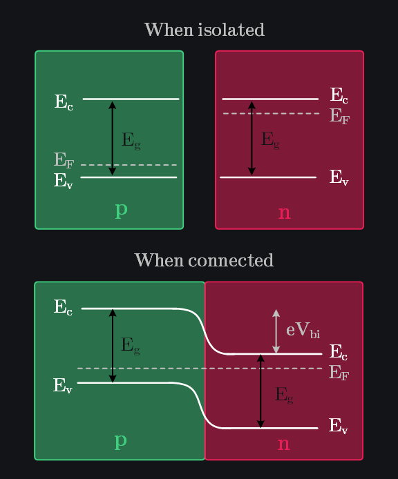
The potential energy of an electron is given by \(E=-e\phi\), meaning electron energy varies as potential varies across the depletion region. As electrons diffuse from the n-region to the p-region, they move along the electric field, gaining potential energy. Although electrons naturally move against the electric field (since the electric field is defined from positive to negative), the diffusion force pushes them along the field, meaning work is done on them, which they store as potential energy. Since band diagrams represent electron potential energy, this is reflected in the upward bending of the conduction band in the p-region. As electric field continues to build up, it opposes further electron diffusion from n to p, at one point completely stopping it, thus creating an energy barrier. This results in the conduction band bending downward in the n-region.
Thus, the energy-band diagram of a PN junction takes on the characteristic bent shape, with the difference in conduction band edges between the p-type and n-type regions equal to \(eV_{bi}\). The valence band also bends since the bandgap remains unchanged—doping or junction formation does not alter the material’s intrinsic bandgap. While the conduction and valence bands bend due to the built-in field, the Fermi level remains flat because the system (p and n materials both as “one”) is in equilibrium. This ensures that the electron and hole concentrations are correctly represented —\(E_F\) being close to \(E_c\) in the n-region (indicating high electron concentration) and close to \(E_v\) in the p-region (indicating high hole concentration).
5.3 PN Junction Under Forward Bias
5.3.1 Lowering of Barrier
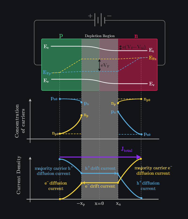
When a forward bias voltage \(V_F\) is applied (p-side at higher potential than n-side), it reduces the built-in potential across the junction. The conduction band on the p-side shifts downward because the applied voltage (+ive on p-side) raises the potential \(\phi\), lowering electron energy (as \(E=-eV\)). Similarly, the conduction band on the n-side shifts upward because applied potential (-ive on n-side) raises electron energy. The overall result is a lowering of the barrier, which allows electrons to be more easily injected from n to p and holes from p to n, leading to the current flow.5.3.2 Excess Minority Carriers
When forward-bias voltage lowers the potential barrier and let majority carrier electrons from the n-side travel across the junction into the p-side, the minority carrier electron concentration increases in p-side near the edge of depletion. This means there are now “excess” minority carrier electrons in the p-side. Similarly, there would be excess minority carriers (i.e., holes) in n-side. Concentration of excess minority carriers can be given as:
where,
- \(n_p\) is excess electron concentration at the edge of depletion region in p-side
- \(n_{p0}\) is thermal-equilibrium concentration of minority carrier in p-side (i.e., the default concentration without any forward bias)
- \(p_n\) is excess hole concentration at the edge of depletion region in n-side
- \(p_{n0}\) is thermal-equilibrium concentration of minority carrier in p-side (i.e., the default concentration without any forward bias)
Note in image below, you will see two \(n_p\) (and two \(p_n\)), and their concentration is different on two edges of depletion region, this is because some recombination happened here. More on this below.
5.3.3 Split of Fermi Levels
The injection of minority carriers changes the minority carrier concentration, but the majority carriers remain same. How can we represent electron and holes concentration using Fermi level now? For example, let’s think of injected electrons in n-side. If you were to try to represent both electrons and holes in n-side with a single Fermi level, you’d have to shift that level closer to the conduction band to account for the increased electrons. But doing so would erroneously suggest a reduction in the hole concentration, which would be incorrect. Therefore, we define a separate quasi-Fermi level for electrons to accurately describe their elevated density, while the holes quasi-Fermi level remains near the valence band. This separation into two quasi-Fermi levels allows us to properly represent the non-equilibrium conditions under forward bias: one quasi-Fermi level (\(E_{Fn}\)) for the electrons, and another (\(E_{Fp}\)) for the holes.
5.3.4 Current Flow (Big Picture)
Now that excess minority carriers have made it through junction, how do they flow to the other end of device and go back to applied voltage source? A: they diffuse again! Let’s revise by tracking electron current starting from n-side. Applied voltage source injected more electrons to n-side. Electrons flow from here to depletion region edge through diffusion. In the depletion region, since barrier is lowered by applied voltage source, electrons get swept to the other side by drift under electric field. As they make it out of depletion region to the p-side, they find them in “excess” (because p-side had them in minority). So, these excess electrons diffuse again. Same story with hole current from p-side. Therefore, total current through PN junction is sum of electrons and holes current and is constant along the x-axis although it changes hands (diffusion to drift to diffusion) as shown in image below.
5.3.5 Carrier Concentrations Explained
In the image above, the injected minority carrier concentration decays as you move away from the depletion region. This makes sense because the highest concentration occurs at the depletion edge, where excess carriers are injected. As they diffuse further, they gradually recombine with majority carriers, leading to a steady decrease in their concentration. On the other hand, the majority carrier concentration remains nearly unchanged, even though recombination is occurring. This is because majority carriers vastly outnumber minority carriers (by several orders of magnitude), so the recombination of a small fraction of them has a negligible impact on their overall density. However, despite the majority carrier concentration appearing nearly constant, a small but crucial gradient exists between the contact and the depletion edge. This slight difference is enough to drive a significant diffusion current, which is why, in the image above, the majority carrier concentration seems to change only slightly, yet the diffusion current is substantial.5.3.6 Not All Injected Carriers Make It
- Not all minority carriers injected make it to the far edge of device (where contact is placed) to contribute to the current because some of them recombine with majority carriers as we noted earlier. Therefore, it is crucial to minimize diffusion length (by lowering doping) or make sure the length of neutral n and p sides is small to reduce recombination.
- Electrons injected from n-side and holes injected from p-side in depletion region recombine leading to additional loss of current. To reduce this recombination, higher forward bias voltage is required which makes depletion region narrow. With a smaller volume available for recombination, fewer carriers recombine in the depletion region, and more are injected.
Ideally, we want to minimize recombination to improve current “collection” efficiency that is all the current injected (emitted) should be collected – hmm did you connect the dots yet? See where the terms emitter and collector come from in BJT.
5.3.7 Current Equation
Current through PN junction can be approximated as:
where,
\[ V_T=\frac{kT}{q} \]
and \(I_S\) is reverse saturation current. More on this below.
We can also determine what forward bias voltage is needed for given current:
\[ V_F \approx V_T \, ln \left[ \frac{I_D}{I_S} \right] \]
5.3.8 High Level Injection (just in case you know)
In the derivation of the ideal diode I–V relationship, low-level injection is assumed. Low injection implies that the excess minority carrier concentrations are always much less than the majority carrier concentration. However, as the forward-bias voltage increases, the excess carrier concentrations increase and may become comparable or even greater than the majority carrier concentration. This is called high-level injection. This causes the quasi-Fermi levels for electrons and holes to move closer together, significantly altering the carrier distribution and increasing the conductivity of the region which is known as conductivity modulation. As a result, the effective resistance of the device decreases and the current no longer follows the exponential relation.
5.4 PN Junction Under Reverse Bias
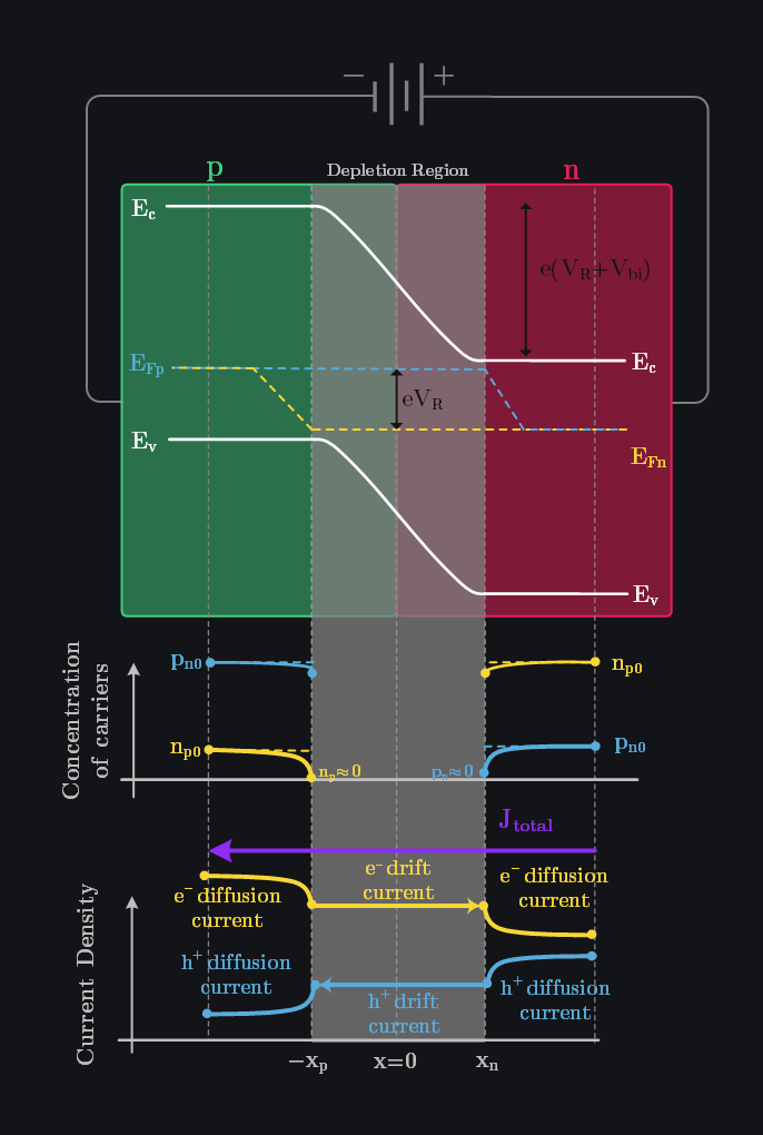
When a reverse bias voltage \(V_R\) is applied (p-side at lower potential than n-side), it “adds” into the built-in potential across the junction. The electric fields in the neutral p and n regions are essentially zero, or at least very small, which means that the magnitude of the electric field in the depletion region must increase above its thermal-equilibrium value due to the applied voltage, leading to a higher barrier and lower current. (You can also apply similar logic as we did for forward bias that is the applied potential raising electron energy in p-side and reducing it in n-side, thus resulting in further bending of energy band)Reverse bias current has two components (other than leakages like tunneling etc.)
1. Reverse Saturation Current: It is due to thermally generated minority carriers in the neutral p & n regions which are near the depletion region and get swept across by the depletion region by strong electric field. For example, a hole in n-region gets swept to p-region. Now, holes were already in majority in p-side, but this newly injected hole creates a small concentration gradient and diffuse to the far end of p-region thus completing the current flow. This is the dominant reverse bias current at low reverse bias voltages and independent of reverse bias voltage itself. It can be given as:
where,
- \(A\) is the junction area
- \(L_n\) and \(L_p\) are the minority carrier diffusion lengths for electrons and holes, respectively.
2. Reverse Bias Generation Current: Although concentration of electrons and holes is essentially zero within the depletion region (because it was depleted of carriers, remember?), some electron-hole pairs are still thermally generated in the depletion region due to mid-gap trap states (defects or impurities). They are swept out of the space charge region by the electric field and contribute to additional reverse bias current. This current can start becoming significant at moderate reverse bias voltages and is directly proportional to depletion region width (and hence to the reverse bias voltage applied).
where,
- \(W\) is the depletion region width,
- \(n_i\) is the intrinsic carrier concentration,
- \(\tau_0\) is the average of electron and hole lifetime.
3. High Reverse Bias Current: Avalanche and Zener reverse bias currents are dominant at higher reverse bias voltages and may even lead to breakdown to junction. More on this in PN junction breakdown section.
5.5 PN Junction Capacitance
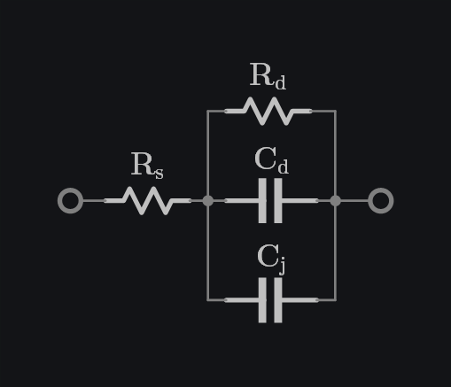
PN junction has two parasitic capacitances: 1) Depletion capacitance (dominant in reverse bias), and 2) Diffusion capacitance (dominant in forward bias).
5.5.1 Junction or Depletion Capacitance
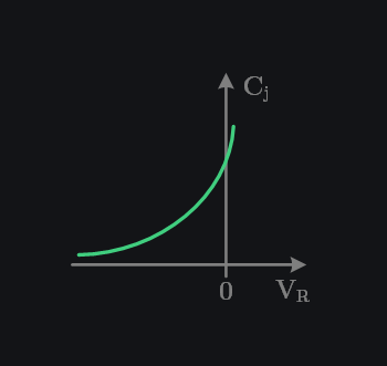
Since we have a separation of positive and negative charges in the depletion region, a capacitance is formed between p and n-side, known as depletion capacitance. This capacitance itself is parasitic, and one would like to avoid in circuit design, but reverse-biased pn junctions exhibit a unique property that becomes useful in circuit design. As \(V_R\) increases, so does the width of the depletion region, revealing that the capacitance of the structure decreases as the two plates move away from each other. The junction therefore can be used as a voltage-dependent capacitor.
It can be shown that the capacitance of the junction per unit area is equal to:
\[C_j = \frac{C_{j0}}{\sqrt{1+\dfrac{V_R}{V_{bi}}}}\]
where \(\varepsilon\) represents the dielectric constant of material.
Why Does the Depletion Region Width Increase with Increase in Reverse Bias Voltage?
When a reverse bias voltage \(V_R\) is applied, it adds into the built-in potential across the junction increasing electric field \(E\). A higher \(E\) can be sustained only if a larger amount of fixed charge is provided (Gauss’s law), requiring that more acceptor and donor ions be exposed and, therefore, the depletion region be widened.
5.5.2 Diffusion Capacitance
We learned that when PN junction is forward biased, an excess minority carrier concentration exists at the edges of depletion region which then diffuses and recombines on its way. We also observed that concentration of these minority carriers depends on forward bias voltage. What happens if you suddenly change forward bias voltage from \(V_{F1}\) to \(V_{F2}\)? The minority carrier concentration will not be able to change instantly as there is a finite minority carrier lifetime that excess minority carriers need to recombine and reflect “new” excess concentration governed by \(V_{F2}\). This is as if there is storage of charge, that does not respond to instantaneous voltage change and takes time to reflect. This is the characteristic of a capacitance! Therefore, we name this behavior as diffusion capacitance and also call minority carrier lifetime as storage time. If \(Q\) is the stored charge and \(I\) is the forward bias current, we can define diffusion capacitance \(C_d\) to be:Thus, a longer storage time (or minority carrier lifetime) results in a larger diffusion capacitance, indicating the slower switching speed.
5.6 Small Signal Model
Small signal model of PN junction has depletion capacitance (\(C_j\)), diffusion capacitance (\(C_d\)), series resistance from finite doping of n and p regions (\(R_s\)) and small-signal resistance from I-V curve (\(R_d\)) also called as diffusion resistance.
Expressions for \(C_d\) and \(C_j\) have been define before. \(R_d\) can be defined as:
We have seen minority carrier lifetime poses a fundamental tradeoff in PN junction design:
- Increase lifetime and you will have less recombination which will lead to higher current (and smaller \(R_d\)) for given forward bias voltage.
- Decrease lifetime and you will have lesser diffusion capacitance which will lead to faster switching speed.
5.6.2 Fundamental Trade-off Between Speed and Breakdown
Increasing the doping in the neutral p and n regions lowers the series resistance (\(R_s\)) and minority carrier lifetime (\(\tau_0\)), which in turn lowers the diffusion capacitance (\(C_d\)). Thus, PN junction’s switching speed improves because of reduced RC time constant. However, higher doping leads to a narrower depletion region width which results in lower breakdown voltage (discussed more in section below) and higher depletion capacitance(\(C_j\)). This capacitance is less dominant during forward bias (where diffusion capacitance is the main contributor) and therefore does not affect speed to the first order. Thus, while higher doping enhances speed, it does so at the expense of breakdown voltage, and this compromise must be balanced based on the device’s intended application (i.e., dope higher for high-speed device and dope lower for high-voltage device).
5.7 PN Junction Breakdown
Breakdown due to high voltage (and hence a high electric field) can occur in any material. In a PN junction, it occurs through one of two possible mechanisms: (1) the Zener effect and (2) the avalanche effect.5.7.1 Zener Breakdown
Zener breakdown occurs in highly doped PN junctions through a tunneling mechanism. In a highly doped junction, depletion width is very small, and a high reverse bias bends the band so much that tunneling barrier width (the distance an electron needs to quantum tunnel through) becomes very small, and hence electrons may tunnel directly from the valence band on the p side into the conduction band on the n side. This leads to a sharp current increase breaking down the junction.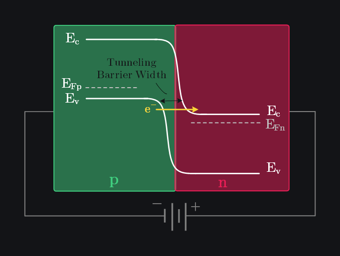
5.7.2 Avalanche Breakdown
In most PN junctions, the predominant breakdown mechanism is the avalanche effect because doping levels are moderate to low (\(<10^{15}\,cm^{3}\)). Avalanche breakdown occurs when electrons and holes moving across the depletion region experience a very high electric field, causing them to accelerate significantly. As they gain energy, they collide with atomic electrons, breaking covalent bonds and generating additional electron-hole pairs. These newly generated carriers can, in turn, accelerate and create further collisions, initiating a chain reaction. This multiplication process leads to a gradual increase in current, which, if uncontrolled, can escalate into a full avalanche breakdown, resulting in excessive current flow and potential destruction of the junction.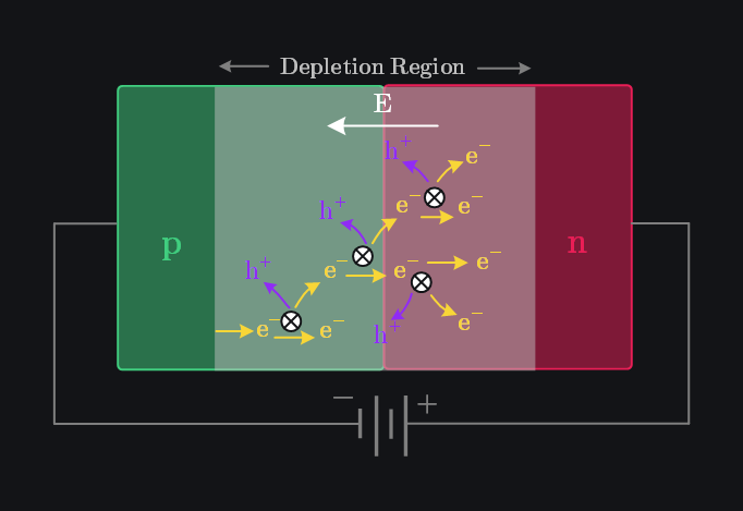
Why Does Zener Breakdown Voltage Decrease with Temperature but Avalanche Breakdown Voltage Increases?
Zener breakdown voltage decreases with temperature because the bandgap energy reduces as temperature increases, making it easier for electrons to tunnel. This reduces the required reverse voltage for breakdown. In contrast, avalanche breakdown voltage increases with temperature due to several factors: 1) Increased lattice vibrations with temperature scatter carriers more frequently; making it harder for them to gain enough energy to break covalent bonds; 2) Higher intrinsic carrier concentration at higher temperature leads to increased recombination, reducing the number of carriers available for impact ionization; 3) Reduced carrier mobility at higher temperature lowers their acceleration, making it more difficult for them to reach the high-energy states necessary for initiating the avalanche process.
As a result, Zener breakdown occurs more easily at higher temperatures, while avalanche breakdown becomes more difficult. This opposite behavior can be exploited to design temperature-compensated diodes, where Zener and avalanche effects contribute equally, resulting in a near-zero temperature coefficient. Such diodes (known as Zener diodes) provide a stable breakdown voltage over a wide temperature range, making them ideal for precision voltage regulation in circuits.
Let’s put two PN junctions back-to-back and see how they form a transistor. But before we do that, let’s take a step back and explore the fascinating, often bumpy journey of its invention. The road to the transistor was anything but straightforward—so much so that it even made someone to say (as later reported by Shockley himself*):
“You know, I might have quit on my research that finally paid off, if I hadn’t read Shockley’s article on how slow he was and how he missed the junction transistor’s key concepts so many times. If he was that dumb, I figured I should stick with it and not give up.”
What struggles and breakthroughs led to one of the most important inventions of the modern era? Let’s uncover the story in the next chapter.
References
“Semiconductor Physics And Devices: Basic Principles” by Donald A. Neamen
“Fundamentals of Microelectronics” by Behzad Razavi
*W. Shockley, “The path to the conception of the junction transistor,” in IEEE Transactions on Electron Devices, vol. 23, no. 7, pp. 597-620, July 1976
Browse by Tags
RFInsights
Published: 24 Feb 2025
Last Edit: 24 Feb 2025